Innovations in Wafer Growth: The Path to Smaller and More Efficient Chips
The semiconductor industry continues to evolve with groundbreaking innovations in wafer growth, paving the way for smaller and more efficient chips. As we delve into the intricacies of wafer level packaging, advanced semiconductor manufacturing, the emergence of integrated chiplets, and the scaling of transistor counts, we uncover the technological advancements that are revolutionizing the way we approach chip integration and design. This article explores these innovations and their implications for the future of semiconductor technology.
Key Takeaways
- Wafer Level Packaging (WLP) has revolutionized chip integration by packaging ICs on the wafer before dicing, leading to smaller and ready-to-use chips, despite thermal management challenges.
- Advanced semiconductor manufacturing methods, including WLP and 3D stacking, are expanding market share by offering compact footprints, improved efficiency, and cost-effectiveness.
- The shift from 2D to 3D system integration through chiplets and Through Silicon Vias (TSV) is a paradigm shift, enabling vertical stacking for performance optimization and miniaturization.
- The increase in vertical connection density is driving the transistor count in GPUs, with the potential to scale toward a trillion transistors through advanced packaging technologies.
- The Mead-Conway moment for 3D integrated circuits reflects a significant leap in IC design complexity, with implications for the future development of semiconductor technology.
Wafer Level Packaging: Revolutionizing Chip Integration
The Evolution of Wafer Level Packaging
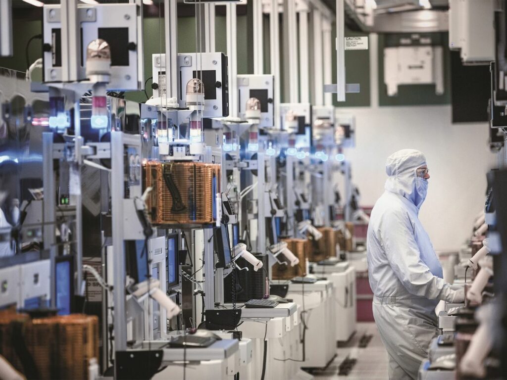
Wafer Level Packaging (WLP) represents a significant shift in semiconductor packaging, moving away from traditional methods like wire bonding and flip-chip. WLP integrates fabrication and testing at the wafer level, streamlining the manufacturing process by packaging entire wafers before dicing. This approach not only enhances efficiency but also reduces costs, making it a cornerstone for the future of chip integration.
The advantages of WLP are evident in its compact design and scalability. Devices utilizing WLP are typically 30-50% smaller than those using conventional packaging techniques. This size reduction is particularly beneficial for mobile, wearable, and IoT devices, where space is at a premium. Moreover, the market share for WLP is on the rise, estimated to be between 12-17%, reflecting its growing adoption across various sectors.
Despite its benefits, WLP faces challenges such as thermal management and increased complexity as the form factor continues to shrink. However, innovations like fan-out techniques are addressing these issues by expanding the number of I/O connections through redistribution layers (RDL), pushing the boundaries of what’s possible with WLP.
Thermal Management and Complexity Challenges
As the density of integrated circuits (ICs) increases and their size decreases, thermal management emerges as a pivotal aspect of semiconductor packaging. The quest for improved electrical performance, coupled with the demand for smaller form factors, adds layers of complexity to this challenge. Ensuring reliability and longevity while managing manufacturing intricacies and cost-reduction pressures further complicates the scenario.
The advent of Wafer Level Packaging (WLP) marked a significant shift in the packaging process, bringing it directly to the wafer. This innovation means that chips are ready for use immediately after dicing, rather than being bare dies. However, the benefits of WLP come with their own set of hurdles, including thermal management and the complexities associated with miniaturization. To address these, the industry has turned to novel solutions such as fan-out techniques, which expand the number of input/output (I/O) connections by utilizing redistribution layers (RDL).
The table below summarizes the key challenges and the corresponding innovations in thermal management and complexity within semiconductor packaging:
| Challenge | Innovation |
|---|---|
| Heat Dissipation | Advanced Thermal Materials |
| Electrical Performance | Novel Circuit Topologies |
| Form Factor Reduction | Heterogeneous Integration |
| Reliability & Longevity | Improved Substrates |
| Manufacturing Complexity | Fan-Out Techniques & RDL |
Understanding these challenges and innovations is crucial for navigating the dynamic landscape of semiconductor packaging. As we continue to push the boundaries of what’s possible, thermal materials and circuit designs will undoubtedly evolve to meet the ever-increasing demands of advanced packaging.
Fan-Out Techniques and Redistribution Layers
The advent of fan-out techniques has marked a significant leap in wafer-level packaging (WLP), enabling a more compact footprint and enhanced efficiency. By extending the interconnects beyond the die boundaries, these techniques incorporate redistribution layers (RDL), which are crucial for increasing the number of input/output (I/O) connections. This innovation is particularly beneficial for devices where space is at a premium, such as mobile, wearable, and Internet of Things (IoT) devices.
Despite the clear advantages, the implementation of fan-out techniques comes with its own set of challenges. One of the primary hurdles is the thermal management within the tightly packed structures. As the form factor reduces, dissipating heat efficiently becomes increasingly complex. Moreover, the market share for WLP is estimated to be between 12-17%, indicating its growing but still emerging presence in the semiconductor packaging industry. To address these challenges and capitalize on the potential of WLP, the encapsulation stage has been integrated into the packaging process, ensuring that after dicing, the chip is not merely a bare die but a ready-to-use component.
The table below summarizes the impact of fan-out techniques on semiconductor packaging:
| Feature | Impact |
|---|---|
| Footprint | Reduced by 30-50% |
| Efficiency | Enhanced |
| Market Share | 12-17% |
| Complexity | Increased |
As the industry continues to evolve, overcoming these hurdles will be crucial for the widespread adoption of fan-out panel-level packaging and the continued miniaturization of semiconductor devices.
Advanced Semiconductor Manufacturing: Beyond Traditional Techniques
The Rise of Non-Traditional Manufacturing Methods
The relentless pursuit of enhanced performance and the need to meet escalating demands have catalyzed the evolution of advanced semiconductor manufacturing. This term broadly refers to a suite of non-traditional manufacturing techniques that diverge from conventional methods, such as wire-bonding and flip-chip. These innovative approaches include, but are not limited to, Wafer Level Packaging, 2.5D stacking, and 3D stacking, which represent the vanguard of semiconductor packaging technology.
Among the plethora of advanced techniques, one particularly noteworthy development is Additively Manufactured Electronics (AME). Although still nascent, AME stands out for its ability to produce highly customized circuits on demand. The technology is rapidly advancing, signaling a potential paradigm shift in how we approach the manufacturing of electronic components.
The following table summarizes the primary categories of advanced manufacturing, highlighting their introduction into the market and their growing significance:
| Technique | Introduction Period | Significance |
|---|---|---|
| Wafer Level Packaging | Last two decades | High |
| 2.5D Stacking | Recent years | Medium |
| 3D Stacking | Recent years | High |
| AME | Emerging | Medium |
As we continue to explore these advanced manufacturing processes, we delve deeper into the intricacies and implications they hold for the future of semiconductor technology.
Impact of Advanced Manufacturing on Market Share
The semiconductor industry has witnessed a significant shift with the advent of advanced manufacturing techniques. These modern methods, which diverge from traditional manufacturing processes, have been instrumental in reshaping market dynamics. Advanced manufacturing, including Wafer Level Packaging (WLP), 2.5D stacking, and 3D stacking, now accounts for approximately 30% of the market share. This segment is characterized by its focus on miniaturization and improved performance metrics.
The market share distribution reflects the ongoing U.S.-China Chip War, where intellectual property and manufacturing capabilities are pivotal battlegrounds. Wire-Bonding, despite being a more established technique, maintains a substantial 20% market share due to its cost-effectiveness in mass production. However, the drive for higher throughput and the need to outpace competitors have led companies to invest heavily in advanced manufacturing. This investment is not just a bid for immediate gains but a strategic move to secure long-term market dominance.
| Technique | Market Share |
|---|---|
| Wire-Bonding | 20% |
| Advanced Manufacturing | 30% |
The table above succinctly captures the market share of different semiconductor manufacturing techniques. As the industry continues to evolve, the impact of these advanced methods on market share is expected to grow, further intensifying the competition among global semiconductor giants.
Encapsulation and Its Role in Efficiency
Encapsulation in wafer-level packaging (WLP) represents a pivotal advancement in semiconductor packaging, offering a compact footprint and enhanced efficiency. By integrating the packaging process at the wafer stage, chips are protected and prepared for use immediately after dicing, eliminating the need for additional packaging steps. This innovation not only streamlines manufacturing but also contributes to the miniaturization of electronic devices.
The encapsulation process has been instrumental in the scalability and cost-effectiveness of WLP, with market share estimates for this technology ranging from 12-17%. The table below highlights the impact of encapsulation on packaging efficiency:
| Feature | Benefit |
|---|---|
| Size Reduction | 30-50% smaller than traditional packages |
| Market Share | Estimated 12-17% |
| Device Suitability | Ideal for mobile, wearable, IoT devices |
Encapsulation also plays a crucial role in the integration of various materials into the substrate, allowing for heterogeneous integration within packages. This leads to an improved functionality-footprint ratio, which is a key driver in the industry. As the demand for smaller, more powerful devices continues to grow, encapsulation will remain an essential component in the evolution of semiconductor packaging.
The Emergence of Integrated Chiplets
From 2D to 3D System Integration
The leap from 2D to 3D system integration marks a significant milestone in the evolution of semiconductor technology. This transition is not just about stacking layers; it’s about creating a new dimension of connectivity and functionality. The 2.5D stacking technique serves as a bridge in this evolution, utilizing an interposer to enable high-density routing between multiple dies before they are packaged into a single chip component.
The benefits of 3D integration are manifold, offering not only a reduction in the physical footprint of chips but also improvements in performance and energy efficiency. Shorter inter-chip connections translate to faster data transfer rates and lower power consumption. Here’s a quick comparison of 2D and 3D integration:
| Feature | 2D Integration | 3D Integration |
|---|---|---|
| Connectivity | Limited by planar space | Enhanced by vertical stacking |
| Performance | Constrained by longer interconnects | Boosted by shorter interconnects |
| Power Efficiency | Higher consumption | Reduced consumption due to proximity |
| Physical Footprint | Larger | Compact due to vertical expansion |
As we continue to push the boundaries of what’s possible with chip design, the shift towards 3D integration is a clear indicator of the industry’s commitment to innovation and efficiency. The implications for future devices are profound, with the potential for more powerful, compact, and energy-efficient electronics reshaping our technological landscape.
The Role of Through Silicon Vias in Miniaturization
Through Silicon Vias (TSVs) have emerged as a cornerstone in the quest for chip miniaturization. These microscopic conduits penetrate silicon wafers, enabling vertical stacking of semiconductor devices. The result is a dramatic reduction in connection lengths, which translates to lower latency and reduced power consumption—key advantages for sectors like AI and high-performance computing.
The compact nature of TSV-enabled devices is particularly beneficial for products where space is at a premium, such as wearables and augmented reality tools. Despite its current niche market share, the technology is expanding, with advancements in TSVs driving this growth. However, the industry must navigate challenges including cost, complexity, and thermal management to fully leverage the potential of 3D stacking.
Recent developments in 3D System-on-Chip (SoIC) technology suggest a promising future. Innovations such as hybrid bonding offer a denser and more efficient alternative to traditional High Bandwidth Memory (HBM) structures, allowing for multi-layered chip stacks with minimal thickness. As the industry continues to refine these techniques, the density of vertical interconnections is poised to increase significantly, paving the way for a new era of semiconductor design.
Interconnect Density and Its Future Potential
The relentless pursuit of miniaturization in semiconductor technology has led to a significant increase in vertical connection density, a trend that mirrors the exponential growth of transistors in GPUs. The potential for interconnect density to grow by an order of magnitude presents a transformative opportunity for chiplet integration in 3D stacks.
As we look toward the future, several challenges and opportunities stand out:
- Thermal management: As interconnect density increases, effective heat dissipation becomes crucial.
- Electrical performance: Balancing the reduction in form factor with improved electrical efficiency is key.
- Cost and complexity: Innovations must address economic viability and manufacturing intricacies.
- Reliability and longevity: Ensuring the durability of denser interconnects is essential.
The market share for technologies enabling 3D stacking, such as Through Silicon Vias (TSV), is currently modest but expanding. The integration of these technologies is critical for applications demanding lower latency and reduced power consumption, such as AI and high-performance computing. The future of interconnect density not only holds the promise of further miniaturization but also the potential to revolutionize the functionality and efficiency of next-generation devices.
Scaling Toward a Trillion Transistors
The Correlation Between Vertical Connection Density and Transistor Count
The relentless pursuit of miniaturization in semiconductor technology has led to a remarkable trend: the vertical connection density in 3D chips has been scaling in tandem with the transistor count in GPUs. This parallel growth is a testament to the industry’s innovation, as it moves beyond the limitations of Moore’s Law, which has been the guiding principle for decades.
Vertical integration through technologies like Through Silicon Vias (TSV) has been pivotal in this advancement. TSVs allow for the vertical stacking of chips, which not only optimizes performance but also aids in the crucial miniaturization of components. The result is a system with minimal connection lengths, lower latency, and reduced power consumption—factors that are especially beneficial for AI and high-performance computing applications.
As we look to the future, the potential for further increasing interconnect density is substantial. Industry experts suggest that there is no foreseeable barrier to expanding the interconnect density by an order of magnitude or more. Such an increase would be instrumental in achieving the ambitious goal of integrating a trillion transistors on a single chip, paving the way for unprecedented computational power and efficiency.
Advanced Packaging Technologies Driving Performance
The relentless pursuit of miniaturization and performance in semiconductor devices has led to significant advancements in advanced packaging technologies. These innovations are not just about scaling down; they’re about smartly integrating various components to enhance the overall system performance. For instance, the concept of system-technology co-optimization (STCO) is pivotal, separating GPU components into chiplets and optimizing each using the most suitable technologies.
Advanced molding equipment (AME) is another breakthrough, promoting miniaturization through highly customized designs. AME supports the integration of diverse materials, enabling heterogeneous integration within packages. This integration is key to improving the functionality-footprint ratio, a vital metric in the industry. However, the path to widespread adoption of AME is fraught with challenges such as ensuring quality, reliability, standardization, and cost-effectiveness.
Despite these challenges, the industry is making strides in overcoming them. Quality and reliability are seeing promising developments, efforts towards standardization are underway, and strategies for cost reduction are being actively pursued. The future of semiconductor packaging is leaning towards on-demand customization and heightened performance, thanks to these technological strides.
System-Technology Co-Optimization for Next-Gen GPUs
The relentless pursuit of higher performance in next-generation GPUs is driving the need for innovative approaches to design and integration. System-technology co-optimization (STCO) is emerging as a pivotal strategy in this arena. By tailoring the architecture of GPU chiplets to their specific functions and optimizing them with the most suitable technologies, we can achieve unprecedented levels of efficiency and performance.
The concept of STCO is not just theoretical; it’s already being applied in the industry. For instance, advanced packaging technologies such as CoWoS (Chip-on-Wafer-on-Silicon) have been instrumental in the development of high-performance GPUs. These technologies facilitate the integration of a large number of transistors by connecting multiple chips in either 2.5D or 3D configurations, pushing the boundaries of what’s possible within the confines of a single chip.
To illustrate the impact of STCO and advanced packaging on GPU development, consider the following table showing the progression of transistor counts in recent GPU models:
| GPU Model | Transistor Count (billions) |
|---|---|
| Nvidia Ampere | 54 |
| Nvidia Hopper | 80 |
As we continue to innovate, the goal of reaching a trillion-transistor GPU becomes more tangible. This leap forward will not only be a milestone for the semiconductor industry but also a testament to the synergy between system design and technological advancement.
A Mead-Conway Moment for 3D Integrated Circuits
Understanding the Mead-Conway Innovation in IC Design
The Mead-Conway innovation, spearheaded by Lynn Conway and Carver Mead in the late 1970s, marked a pivotal moment in the history of integrated circuits (ICs). Their approach to very large scale integration (VLSI) design democratized the process, enabling a broader range of engineers to participate in IC design. By introducing a set of standardized design rules, they abstracted the complexities of semiconductor fabrication, allowing designers to focus on the architecture without deep knowledge of the underlying process technology.
This paradigm shift not only simplified the design process but also paved the way for the development of more complex and powerful chips. As a result, the Mead-Conway methodology became a cornerstone in the evolution of semiconductor design, influencing subsequent generations of IC development.
The table below outlines the key contributions of the Mead-Conway innovation to IC design:
| Aspect | Contribution of Mead-Conway Innovation |
|---|---|
| Design Democratization | Enabled broader participation in IC design |
| Standardization | Introduced a set of design rules for VLSI |
| Complexity Abstraction | Separated design from fabrication complexities |
| Influence on Industry | Became a foundational methodology for IC development |
Implications for 3D IC Development
The Mead-Conway innovation, which revolutionized IC design in the 1970s by standardizing the design process and tools, has profound implications for the development of 3D integrated circuits (ICs). The shift towards 3D ICs represents a paradigm change in semiconductor design, where the focus is not only on the horizontal plane but also on the vertical integration of components.
The benefits of 3D ICs are numerous, including increased performance, reduced power consumption, and a smaller footprint. However, the transition to 3D ICs also introduces new challenges:
- Thermal management becomes more complex as the vertical stacking of components can lead to higher heat density.
- Electrical performance must be optimized without compromising the reduced form factor.
- Manufacturing complexity escalates with the need for precision in stacking and connecting multiple layers.
To address these challenges, a co-design approach is essential, integrating architecture, chip, and package design. This approach is exemplified by the 2.5D IC design, which serves as a stepping stone towards full 3D integration. The table below summarizes the key aspects of transitioning to 3D ICs:
| Aspect | 2D ICs | 2.5D ICs | 3D ICs |
|---|---|---|---|
| Interconnect Density | Low | Medium | High |
| Thermal Management | Manageable | Complex | Highly Complex |
| Electrical Performance | Standard | Optimized | Highly Optimized |
| Manufacturing Complexity | Standard | Increased | Highly Increased |
As we continue to push the boundaries of transistor count, reaching toward a trillion transistors, the role of advanced packaging technologies and system-technology co-optimization (STCO) will become increasingly critical. These advancements will not only drive performance but also dictate the economic viability of future semiconductor products.
The Future of Semiconductor Design Complexity
As the semiconductor industry ventures beyond the familiar confines of traditional scaling, a new era of design complexity emerges. The push for miniaturization and performance optimization is not just a trend but a necessity, driving the industry into the realm of 3D system integration and advanced packaging technologies. This shift marks a significant departure from the past 50 years of semiconductor development, which focused on shrinking the transistor size within a well-defined path.
The future of semiconductor design is characterized by a convergence of disciplines. Chip designers, system architects, and manufacturers must now possess a holistic understanding of chip technology, 3D IC technology, and advanced packaging. The development of a common language for these technologies is crucial, enabling electronic design tools to comprehend and facilitate the design process for complex 3D IC systems.
The semiconductor packaging industry, at this crossroads, witnesses significant growth, with techniques like 3D stacking and Wafer Level Packaging (WLP) capturing a substantial market share. The table below highlights the market share captured by advanced manufacturing techniques:
| Technique | Market Share |
|---|---|
| 3D Stacking | 15% |
| WLP | 15% |
In conclusion, the semiconductor industry is at the threshold of a new chapter where the integration of chiplets and the rise of 3D system integration will redefine what is possible. The journey ahead is filled with opportunities and challenges, but the potential for innovation is boundless.
CONCLUSION
As we stand on the precipice of a new era in semiconductor technology, the innovations in wafer growth and chip manufacturing are leading us towards an incredibly compact and efficient future. The transition from integrated devices to integrated chiplets, the rise of advanced manufacturing techniques such as Wafer Level Packaging (WLP) and 3D stacking, and the relentless pursuit of miniaturization have all contributed to a seismic shift in the industry. With the potential to achieve a trillion transistors on a chip and the advent of system-technology co-optimization, the future of semiconductor packaging is not only promising but also indicative of the boundless possibilities that lie ahead. The challenges of thermal management and increased complexity are being met with ingenuity and a forward-thinking approach, ensuring that the semiconductor industry continues to thrive and evolve, driving innovation across multiple sectors from mobile and wearable technology to AI and high-performance computing.
Frequently Asked Questions
What is Wafer Level Packaging (WLP) and how is it changing the semiconductor industry?
Wafer Level Packaging is a process where packaging is applied to entire wafers before dicing, rather than packaging each die individually after dicing. This results in a more compact footprint and enhanced efficiency, making it ideal for mobile, wearable, and IoT devices. WLP is revolutionizing chip integration by allowing for smaller, more cost-effective chips with a higher I/O connection density through techniques such as fan-out and redistribution layers.
What challenges does thermal management pose to wafer level packaging?
As the form factor of chips decreases, thermal management becomes more challenging due to the increased power density and limited space for heat dissipation. Innovations in packaging design and materials are critical to effectively manage heat and maintain chip performance and reliability.
How has advanced semiconductor manufacturing impacted the market?
Advanced semiconductor manufacturing, which includes non-traditional methods like Wafer Level Packaging and 3D stacking, has led to more efficient and powerful chips. This has significantly impacted the market, with these techniques capturing a substantial market share and driving competition, particularly in high-performance computing and AI applications.
What role do Through Silicon Vias (TSVs) play in chip miniaturization?
Through Silicon Vias (TSVs) are small vias that penetrate silicon substrates, enabling vertical stacking of chips. This technology facilitates miniaturization and performance optimization by allowing for shorter connection lengths, lower latency, and reduced power consumption, which is particularly beneficial for AI and high-performance computing.
How will the drive towards a trillion transistors shape the future of semiconductors?
The push towards a trillion transistors on a chip will require significant advancements in vertical connection density and packaging technologies. This will lead to more complex and powerful chips, driving the development of new technologies like system-technology co-optimization (STCO) for next-generation GPUs and other high-performance devices.
What is the significance of the Mead-Conway innovation in IC design, and how does it relate to 3D IC development?
The Mead-Conway innovation revolutionized IC design by standardizing the design process and making it more accessible. This breakthrough is analogous to the current advancements in 3D IC development, which are simplifying the integration of multiple chiplets into a single, efficient system, potentially leading to a new era of semiconductor design complexity.