A Comprehensive Guide to Wafer Level Testing in Chip Manufacturing
Wafer level testing is a critical phase in chip manufacturing, where each semiconductor wafer is meticulously tested for defects and performance before being diced into individual chips. This comprehensive guide delves into the nuances of wafer level testing, exploring fundamental concepts, advanced techniques, integration with yield management, challenges and solutions, and future trends that are shaping the industry. With the advent of technologies like GaN for high voltage devices, machine learning for defect detection, and the influence of 5G and AI on testing protocols, this guide provides insightful knowledge for professionals in the semiconductor field.
Key Takeaways
- Understanding the wafer testing process is foundational for ensuring the quality and reliability of semiconductor devices, particularly with the integration of materials like GaN for high-performance applications.
- Advanced techniques such as machine learning and optical profilometry are revolutionizing defect detection and substrate analysis, leading to more efficient and accurate wafer level testing.
- Effective integration of wafer testing data with yield management systems, such as implementing SPC software, is crucial for identifying yield losses and driving actionable insights for process improvements.
- Addressing the challenges in wafer level testing involves identifying root causes of defects and leveraging software solutions like yieldWerx Enterprise to enhance throughput without compromising quality.
- The semiconductor industry must stay abreast of future trends and innovations, including the impact of emerging technologies like 5G, AI processors, and quantum computing on wafer level testing protocols.
Fundamentals of Wafer Level Testing
Understanding the Wafer Testing Process
Wafer level testing is a critical step in the semiconductor manufacturing process. It involves probing individual semiconductor devices on a wafer to identify defects and confirm functionality before the wafer undergoes further manufacturing steps. This process is essential for ensuring the quality and reliability of the final product.
The testing process typically includes a series of electrical tests that are performed using specialized equipment known as probe stations. These stations are equipped with fine needles, or probes, that make contact with the test pads on the semiconductor devices. The following list outlines the general steps involved in wafer level testing:
- Initial visual inspection to check for any obvious physical defects.
- Alignment of the wafer on the probe station.
- Contacting the device’s test pads with the probes.
- Running electrical tests to measure device characteristics.
- Recording and analyzing the test data to identify any non-conforming devices.
The results from wafer level testing are crucial for determining the next steps in the manufacturing process, such as which devices to package and which to discard. By catching defects early, manufacturers can save on costs and prevent faulty devices from reaching the market.
Key Performance Metrics in Chip Manufacturing
In the realm of chip manufacturing, performance metrics are pivotal for assessing the quality and efficiency of the production process. These metrics not only guide the manufacturing process but also provide insights into the potential areas for improvement. Among the key metrics, the Process Capability Index (CPK) stands out as a statistical measure of a process’s ability to produce output within specified limits. Another crucial metric is the Part Average Test (PAT), which helps in identifying devices that, while not failing, show signs of potential future failure.
To ensure a comprehensive understanding, here’s a succinct table outlining some of the primary performance metrics:
| Metric | Description | Relevance |
|---|---|---|
| CPK | Measures process capability | Indicates the consistency and reliability of the production process |
| PAT | Identifies near-failing devices | Prevents future failures and enhances reliability |
| Yield | Percentage of good units produced | Directly correlates with profitability |
| Throughput | Rate of production | Balances efficiency with quality |
These metrics serve as the foundation for yield enhancement strategies and are integral to maintaining a competitive edge in the semiconductor industry. By closely monitoring and analyzing these metrics, manufacturers can identify trends, pinpoint inefficiencies, and implement corrective actions to optimize the production process.
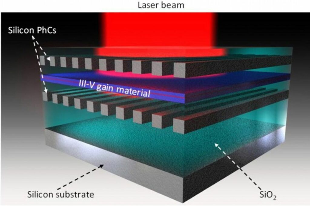
The Role of GaN in High Voltage and Frequency Devices
Gallium Nitride (GaN) has emerged as a transformative material in the realm of high voltage and high frequency power devices. Its inherent properties allow for enhanced efficiency in power converters, as well as reduced conduction and minimal switching losses. This is particularly beneficial in applications where power density and efficiency are critical.
Despite its advantages, GaN devices face challenges related to substrate defects which can impede performance. Studies have shown that surface morphology can significantly affect diode performance in vertical GaN Schottky diodes. To address these issues, researchers are developing computational algorithms and utilizing wafer scale optical techniques to optimize performance and yield.
The table below summarizes key findings from recent studies on GaN device performance:
| Study ID | Focus Area | Key Finding |
|---|---|---|
| Ebrish et al. | Anode doping in GaN diodes | Improved avalanche characteristics |
| Pandey et al. | Edge termination design | Enhanced reliability in P-N diodes |
| Hite et al. | Surface morphology | Correlation with diode performance |
| Gallagher et al. | Computational algorithms | Prediction of high voltage GaN diode quality |
Continued research and development in this area are crucial for realizing the full potential of GaN in advanced semiconductor applications.
Advanced Techniques in Wafer Level Testing
Machine Learning Applications for Defect Detection
The advent of machine learning has revolutionized the field of wafer level testing, particularly in the domain of defect detection. Machine learning models have demonstrated high accuracy rates exceeding 80% in predicting the presence of 0th and 1st order defects, which are critical for ensuring the reliability of electronic devices. These models are adept at forecasting wafer yields with a notable success rate, identifying 6 out of 7 instances correctly.
However, the detection of 2nd order defects remains a challenge. These defects often do not manifest on the surface and require more sophisticated detection methods. By integrating additional input variables from spectroscopic and x-ray techniques, the predictive capability of machine learning models is expected to improve for these elusive defects.
The table below summarizes the performance of machine learning models in defect detection:
| Defect Order | Detection Accuracy | Notes |
|---|---|---|
| 0th Order | High (>80%) | Surface-level defects |
| 1st Order | High (>80%) | Near-surface defects |
| 2nd Order | Limited | Sub-surface defects, requires additional techniques |
As the technology matures, the integration of machine learning in wafer level testing is poised to become a standard practice, offering a more efficient and accurate approach to quality control in chip manufacturing.
Optical Profilometry for Substrate Analysis
Optical profilometry has become an indispensable tool in wafer level testing, providing high-resolution 3D images of the wafer surface. This technique is crucial for detecting morphological defects that can affect the crystal structure and, consequently, the performance of GaN devices. By mapping the full wafer surface, optical profilometry enables the identification of defects that reduce breakdown voltage, offering a data-rich input for machine learning models aimed at wafer screening.
The process involves capturing detailed surface measurements, such as the root mean squared (RMS) roughness and the count of bumps and pits, which are indicative of the wafer’s quality. These parameters are critical for correlating physical surface characteristics with electrical performance, such as breakdown voltage. A study highlighted the pronounced association between rougher samples with more bumps and pits and the formation of defects, underscoring the importance of this analysis.
To illustrate the practical application of optical profilometry data, consider the following table summarizing the correlation between surface roughness and diode performance:
| Region | RMS Roughness | Outliers | Breakdown Voltage Correlation |
|---|---|---|---|
| 1 | Low | Few | High |
| 2 | Moderate | Moderate | Medium |
| 3 | High | Many | Low |
This table reflects the findings from a cluster plot analysis, where devices with fewer outliers and lower RMS roughness exhibited higher breakdown voltages. Such insights are invaluable for improving the manufacturing process and enhancing the overall yield of high-quality semiconductor devices.
Metrology and Defect Data Management
In the realm of wafer level testing, metrology and defect data management play a pivotal role in ensuring the quality and reliability of semiconductor devices. The integration of advanced metrology tools with comprehensive data management systems allows for precise measurement and analysis of wafer features, which is critical for identifying defects and improving yield.
Effective defect data management hinges on the ability to collect, store, and analyze vast amounts of inspection data. This process is facilitated by tools such as Semiconductor Optical Memory Mapping and Wafer Prober Control Modules, which work in tandem to provide detailed insights into the semiconductor manufacturing process. The table below outlines some of the key components involved in this intricate system:
| Component | Function |
|---|---|
| Inspect Image Management | Stores and processes images from inspections |
| Semiconductor Testing Software | Analyzes test data to identify patterns and outliers |
| YieldWerx Enterprise Software | Enhances yield through data-driven decisions |
By leveraging big data analytics and implementing systems like SPC/SBL/SYL for statistical process control, manufacturers can move from Automated Testing System (ATS) data to actionable insights. This transition is crucial for maintaining process capability indices (CPK) within desired limits and rectifying yield issues promptly. The ultimate goal is to achieve a Zero Defect state through meticulous data analysis and continuous improvement strategies.
Integration of Wafer Testing with Yield Management
Correlating Testing Data with Yield Losses
In the semiconductor industry, correlating testing data with yield losses is a critical step towards enhancing production efficiency. By analyzing wafer test results, manufacturers can identify the root causes of yield losses and implement targeted improvements. This process often involves leveraging big data analytics to sift through vast amounts of testing data and pinpoint areas where yield is impacted.
The table below illustrates a simplified example of how testing data can be correlated with yield losses:
| Voltage Cutoff (V) | Predicted Yield (%) | Experimental Yield (%) | RMS Error |
|---|---|---|---|
| 50 | 98 | 95 | 1.2 |
| 600 | 96 | 92 | 1.5 |
| 950 | 94 | 90 | 1.8 |
This data can then be used to refine testing protocols and improve the semiconductor manufacturing process. By employing tools like Statistical Process Control (SPC) and yieldWerx Enterprise Software, manufacturers can monitor and adjust processes in real-time, driving towards the goal of Zero Defect production.
Implementing SPC Software for Process Control
The integration of Statistical Process Control (SPC) software into chip manufacturing workflows marks a significant advancement in process control and quality assurance. Real-time data analysis facilitated by SPC software enables rapid identification of process deviations, fostering prompt corrective actions. This immediacy is crucial in reducing waste, boosting productivity, and ensuring consistent product quality.
Key features of SPC software, such as real-time data collection, advanced statistical analysis, and control chart generation, are instrumental in maintaining stringent process control. These features are outlined in the table below:
| Feature | Function |
|---|---|
| Real-time Data Collection | Captures process data as it occurs |
| Statistical Analysis Tools | Analyzes data to identify trends and anomalies |
| Control Chart Generation | Visualizes process stability and control |
| Process Capability Analysis | Assesses process efficiency and potential improvements |
Continuous improvement is a core principle of SPC software implementation. It necessitates an ongoing review and enhancement of processes based on the software’s feedback. This may include fine-tuning parameters, refining data collection methods, or updating software features to meet the evolving needs of semiconductor manufacturing.
From ATE Data to Actionable Insights
The transition from Automated Test Equipment (ATE) data to actionable insights is a pivotal step in semiconductor manufacturing. By leveraging ATE data, manufacturers can optimize test efficiency and enhance yield management. This process involves several key activities, such as Commonality Analysis, which identifies patterns in defects across different wafers, and Outlier Detection, aimed at spotting units that deviate from normal performance parameters.
To effectively manage and analyze ATE data, a structured approach is essential. Below is a list of critical steps in transforming ATE data into valuable insights:
- Collecting and aggregating ATE data across various test stages.
- Applying statistical analysis tools to interpret complex data sets.
- Generating control charts to monitor and maintain process control.
- Integrating ATE data with other manufacturing and enterprise sources for a comprehensive historical record.
These steps ensure that the vast amounts of data generated during wafer level testing are not only stored but also meticulously analyzed to rectify yield issues and maintain high semiconductor quality.
Challenges and Solutions in Wafer Level Testing
Identifying and Addressing Root Causes of Defects
In the quest to enhance semiconductor yield, identifying and addressing the root causes of defects is paramount. A study has shown that defects causing a significant drop in breakdown voltage often extend through large portions of the device layers, indicating the severity of such imperfections. Optical profilometry has proven effective in detecting these extended defects, which are critical to the device’s performance.
Defects are categorized based on their impact on breakdown performance. Here is a simplified classification:
- 0th order defects: May lead to catastrophic failures.
- 1st order defects: Result in a significant reduction in breakdown performance.
- 2nd order defects: Associated with a milder decrease in breakdown.
Interestingly, higher order defects may exist in well-functioning devices, suggesting a complex relationship between defect types and device performance. The correlation between breakdown voltage and optical profilometry parameters, such as RMS and the number of outliers, is strong, underscoring the importance of these metrics in defect analysis.
Addressing these defects requires a systematic approach, often involving advanced data management and analysis tools. YieldWerx Enterprise Software, for instance, provides a comprehensive suite for yield enhancement that includes modules for defect data management, semiconductor testing, and yield analysis. By leveraging such tools, manufacturers can pinpoint the root causes of yield losses and implement targeted improvements.
Enhancing Throughput without Compromising Quality
In the competitive landscape of chip manufacturing, enhancing throughput is a critical goal that must be balanced with the imperative to maintain high-quality standards. The integration of advanced software solutions has proven to be a key factor in achieving this balance. These solutions enable precise monitoring and analysis, which in turn fosters a more productive manufacturing environment capable of meeting market demands without compromising on quality.
One such solution is the implementation of Statistical Process Control (SPC) software. SPC software is essential for maintaining a competitive edge and ensuring consistent product quality. It empowers manufacturers with data-driven decision-making, which enhances production efficiency and upholds quality standards. YieldWerx is an example of a comprehensive toolset that includes STDF, ATDF, WAT PCM & ATE data analysis, and wafer mapping, all of which are instrumental in optimizing yield and maximizing test efficiency.
The table below outlines the key features of YieldWerx that contribute to throughput enhancement while safeguarding quality:
| Feature | Description |
|---|---|
| In-depth Data Analysis | Supports complex data analysis crucial for high-quality production. |
| Real-time Alerts | Provides immediate notifications for anomalies, enabling swift corrective actions. |
| SPC System | Facilitates process control and consistent quality through statistical analysis. |
| End to End Data Analysis | Integrates various data points for comprehensive oversight. |
YieldWerx Enterprise Software for Yield Enhancement
YieldWerx Enterprise Software plays a pivotal role in semiconductor yield enhancement, offering a suite of tools designed to streamline the yield management process. It provides in-depth data analysis capabilities essential for maintaining high-quality standards in semiconductor production.
Key features of YieldWerx include Statistical Bin Limit (SBL) and Statistical Yield Limit (SYL), which are crucial for setting precise process thresholds and monitoring yield deviations. This functionality is particularly effective for early detection of issues and sustaining optimal yield levels.
The software’s integration and compatibility features allow for seamless incorporation into existing semiconductor manufacturing systems, ensuring efficient data analysis and process control. YieldWerx’s design supports complex data analysis, a significant factor in achieving zero defects in production.
| Feature | Description |
|---|---|
| SBL | Sets precise binning process thresholds |
| SYL | Monitors yield thresholds for early deviation detection |
| Integration | Compatible with existing manufacturing systems |
| Data Analysis | Supports complex analysis for high-quality production |
Future Trends and Innovations in Wafer Level Testing
The Impact of 5G and AI Processors on Testing Protocols
The advent of 5G networks and AI processors is reshaping the landscape of wafer level testing in chip manufacturing. These technologies demand chips that can handle high-speed, low-latency communication and complex algorithms, necessitating a new approach to testing protocols.
5G and AI advancements have led to the development of AI-driven test optimization, which leverages AI to optimize ATPG pattern generation on the gate-level netlist. This innovation not only streamlines the testing process but also significantly reduces production test patterns and associated costs.
The following table highlights the key areas influenced by 5G and AI technologies and their impact on semiconductor testing:
| Area of Influence | Impact on Testing Protocols |
|---|---|
| Communication Chips | Need for high-speed, low-latency testing |
| Power Devices | Efficient power management testing for base stations |
| Autonomous Driving | Reliable testing for safety-critical components |
| IoT Devices | Testing for low-power, always-connected chips |
As the semiconductor industry continues to evolve with these emerging technologies, testing protocols must adapt to ensure that the chips meet the stringent requirements of modern applications.
Emerging Technologies in Semiconductor Testing
The semiconductor industry is witnessing a surge in technological advancements that are reshaping wafer level testing. Cryogenic Probing is one such technology that has gained traction, particularly for its application in quantum computing and low-temperature electronics testing. This technique allows for the characterization of electronic properties at extremely low temperatures, which is critical for the development of next-generation chips.
Another notable advancement is the integration of Machine Learning and AI into testing protocols. These technologies enable the prediction and detection of defects with unprecedented accuracy, thereby reducing the time and cost associated with testing. The table below summarizes some of the key emerging technologies and their applications:
| Technology | Application | Relevance |
|---|---|---|
| Cryogenic Probing | Quantum Computing | High |
| Machine Learning | Defect Detection | Growing |
| Autonomous Semiconductor Test | High Volume Manufacturing | Emerging |
As the complexity of chips increases, with some undergoing up to six stages of testing, the need for efficient and reliable testing methods becomes paramount. The industry is moving towards more autonomous semiconductor test systems that can handle the intricate demands of modern chip manufacturing, from wafer acceptance to final testing stages.
The Evolution of Wafer Level Testing in the Era of Quantum Computing
As the semiconductor industry ventures into the quantum realm, wafer level testing faces unprecedented challenges and opportunities. With quantum processors exceeding the 100-qubit mark, understanding their performance has never been more critical or more difficult. The complexity of quantum devices necessitates innovative approaches to testing, ensuring that the quantum bits (qubits) operate as intended.
The establishment of the Center for Advanced Wafer-Level Packaging Applications and Development marks a significant stride in addressing these challenges. This initiative aims to propel innovation in wafer level testing, particularly for quantum computing applications, by enhancing domestic semiconductor manufacturing capabilities.
The following list highlights key areas of focus in the evolution of wafer level testing for quantum computing:
- Development of specialized cryogenic probing techniques for quantum devices.
- Integration of advanced machine learning algorithms for defect detection and analysis.
- Implementation of metrology and defect data management systems tailored for quantum chip complexities.
- Collaboration with R&D institutions to refine testing protocols for quantum processors.
Conclusion
In summary, wafer level testing is a critical component in the semiconductor manufacturing process, ensuring that chips meet the stringent quality and performance standards required in today’s technology-driven world. Throughout this guide, we have explored the intricacies of wafer level testing, from the importance of detecting outliers with advanced software like yieldWerx to the implementation of SPC software for process control and yield management. As the industry continues to evolve with emerging technologies such as GaN substrates and AI processors, the methodologies and tools discussed here will remain essential for achieving high throughput without compromising quality. For semiconductor manufacturers aiming to maintain a competitive edge and uphold the highest quality standards, embracing these wafer level testing strategies is not just beneficial—it’s imperative.
Frequently Asked Questions
What is wafer level testing in chip manufacturing?
Wafer level testing, also known as wafer probing, is a process where semiconductor devices on the wafer are tested for functionality and performance before being cut into individual chips. This ensures that only working devices proceed to the next stages of manufacturing.
How does GaN technology impact high voltage and frequency devices?
Gallium Nitride (GaN) technology offers superior properties for high voltage and high frequency power devices, such as better thermal performance and higher efficiency. However, substrate defects can affect the optimal performance of vertical devices, necessitating advanced wafer level testing.
What role does machine learning play in wafer level testing?
Machine learning can be applied to wafer level testing to improve defect detection. By analyzing data from techniques like optical profilometry, machine learning algorithms can identify patterns and anomalies that may indicate defects, thus enhancing the testing accuracy.
How is wafer testing integrated with yield management?
Wafer testing data is crucial for yield management as it helps identify the root causes of yield losses. By correlating test data with yield information, manufacturers can implement process improvements and control measures to optimize yield rates.
What are the challenges in wafer level testing and how are they addressed?
Challenges in wafer level testing include identifying root causes of defects and balancing throughput with quality. Solutions like yieldWerx Enterprise Software enable precise monitoring and analysis to enhance throughput without compromising quality.
What future trends are shaping wafer level testing?
The advent of 5G and AI processors is pushing the need for more advanced testing protocols. Additionally, emerging technologies such as semiconductor optical memory mapping and quantum computing are expected to evolve wafer level testing techniques.