A Deep Dive into Wafer Probe Testing
Wafer probe testing might sound complicated, but it’s really just a way to check if tiny parts inside our electronic gadgets work correctly. Imagine testing a toy to see if it works before giving it to someone. This process is super important because it makes sure that our phones, computers, and other devices don’t break easily. Over time, the methods and tools used for wafer probe testing have changed a lot, making the tests faster and more accurate.
Key Takeaways
- Wafer probe testing ensures the tiny parts inside electronics work correctly.
- The methods and tools for testing have evolved to become faster and more accurate.
- Probe card holders play a crucial role in the testing process.
- Different industries like consumer electronics and automotive rely on wafer probe testing.
- Future advancements in technology will continue to improve the testing process.
Understanding Wafer Probe Testing
Definition and Importance
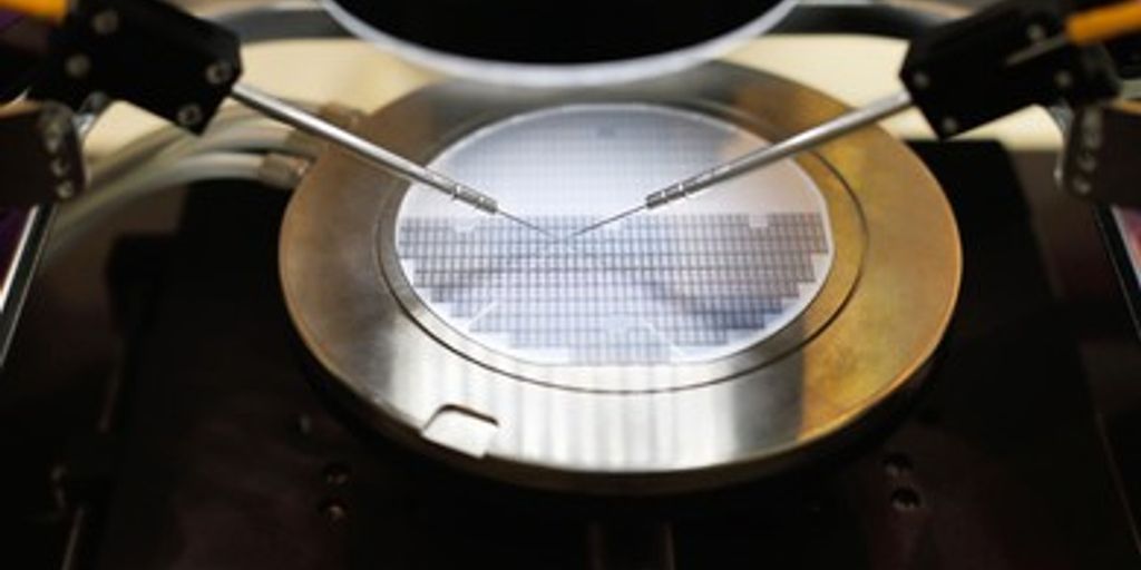
Wafer probe testing is a crucial step in semiconductor manufacturing. It involves checking the electrical performance of individual chips on a wafer before they are cut and packaged. By connecting the test system to the wafer, probe cards enable early detection and elimination of defective chips, ensuring only the best ones move forward in the production process.
Historical Development
The history of wafer probe testing dates back to the early days of semiconductor manufacturing. Initially, testing was done manually, which was time-consuming and prone to errors. Over the years, advancements in technology have led to automated systems that are faster and more accurate.
Key Components Involved
Several key components are involved in wafer probe testing:
- Probe Cards: These are used to make contact with the wafer and test the electrical performance of the chips.
- Probe Card Holders: These ensure precise and consistent contact between the probes and the semiconductor device.
- Test Systems: These systems control the testing process and collect data on the performance of each chip.
Each of these components plays a vital role in ensuring the reliability and performance of electronic devices.
Technological Advancements in Wafer Probe Testing
Modern Techniques
The world of wafer probe testing has seen significant changes with the introduction of modern techniques. One major advancement is the use of automated systems that enhance precision and speed. These systems reduce human error and increase throughput, making the testing process more efficient.
Innovative Materials
As semiconductor technology evolves, the need for more advanced materials in probe card holder construction becomes evident. Researchers are exploring materials with improved conductivity and reduced thermal expansion. These materials help in maintaining stability and accuracy during high-speed testing processes.
Impact on Testing Efficiency
The integration of smart technologies, such as sensors and real-time monitoring, has greatly impacted testing efficiency. These innovations allow for fine-tuning the position of the probe card, ensuring optimal contact between the probes and the semiconductor device. This level of precision is crucial for maintaining the reliability and quality of electronic devices.
Challenges in Wafer Probe Testing
Wafer probe testing is essential in the semiconductor industry, but it comes with its own set of challenges. Testing VCSEL devices on wafers presents multiple challenges. One significant requirement is the ability to perform accurate and reliable tests despite various obstacles.
Role of Probe Card Holders in Wafer Probe Testing
Design and Functionality
Probe card holders are essential in semiconductor testing. They securely hold the probe card in place, ensuring precise contact with the semiconductor device. This precision is crucial because even a tiny misalignment can lead to inaccurate test results, affecting the final product’s reliability.
Material Considerations
The base of a probe card holder is usually made from high-quality materials like stainless steel or other alloys. These materials provide the necessary strength and stability to maintain accurate positioning during testing. Modern holders also use advanced materials and automated systems to enhance performance.
Maintenance and Longevity
Regular maintenance of probe card holders is vital for their longevity. Proper care includes cleaning and checking for wear and tear. Investing in high-quality holders not only improves testing accuracy but also increases productivity and reduces costs in the long run.
Applications of Wafer Probe Testing in Various Industries
Consumer Electronics
In the realm of semiconductor testing, wafer probing plays a pivotal role. Consumer electronics heavily rely on wafer probe testing to ensure the quality and performance of devices like smartphones, tablets, and laptops. This testing helps in identifying defects early, ensuring that only the best products reach the market.
Automotive Industry
The automotive industry demands zero-defect components for safety and reliability. Wafer probe testing is crucial in verifying the integrity of integrated circuits used in vehicles. This ensures that automotive electronics, such as sensors and control units, function flawlessly under various conditions.
Telecommunications
Telecommunications equipment, including 5G technology, requires precise and reliable components. Wafer probe testing ensures that these components meet stringent performance standards. This testing is essential for maintaining the efficiency and stability of communication networks.
| Industry | Key Application Areas |
|---|---|
| Consumer Electronics | Smartphones, Tablets, Laptops |
| Automotive | Sensors, Control Units |
| Telecommunications | 5G Technology, Communication Networks |
Improving Accuracy in Wafer Probe Testing
Calibration Techniques
Calibration is crucial for ensuring the accuracy of wafer probe testing. Regular calibration helps maintain the precision of the probes. This involves adjusting the probe card to align perfectly with the semiconductor device. Calibration mechanisms allow for fine adjustments, ensuring optimal contact.
Error Reduction Strategies
Reducing errors in wafer probe testing is essential for reliable results. Some effective strategies include:
- Implementing automated systems to minimize human error.
- Using high-quality materials for probe cards to ensure durability.
- Regularly maintaining and cleaning the equipment to prevent contamination.
Technological Tools
Advanced technological tools play a significant role in improving accuracy. These tools include:
- Precision motors and sensors for accurate positioning of probe cards.
- Automated arms for rapid and precise adjustments.
- Enhanced thermal management systems to control temperature variations during testing.
Future Trends in Wafer Probe Testing
Emerging Technologies
The semiconductor industry is rapidly evolving, and new technologies are constantly being developed to improve wafer probe testing. One of the most exciting trends is the integration with Industry 4.0 principles. This includes real-time monitoring, data analytics, and predictive maintenance, which are becoming standard features in modern probe card holders. These advancements are ushering in a new era of intelligent semiconductor testing.
Market Predictions
As technology advances, the demand for high-speed semiconductor testing continues to rise. High-quality probe cards and holders, although initially expensive, offer long-term benefits such as improved accuracy and productivity. This leads to overall cost savings in semiconductor testing operations. The market is expected to grow as more industries recognize the importance of investing in advanced testing equipment.
Research and Development
Ongoing research and development are crucial for the future of wafer probe testing. Miniaturization and high-density testing are key focus areas. Engineers are continually working on designing probe card holders with advanced materials to maintain stability and accuracy at elevated testing speeds. This is essential for meeting the increasing demands of modern semiconductor testing.
Conclusion
In summary, wafer probe testing is a vital part of making sure our electronic devices work well and last long. This process checks the tiny parts inside semiconductors to find any problems early on. By doing this, companies can fix issues before the devices reach customers. As technology keeps getting better, so do the tools and methods used in wafer probe testing. This means even more reliable and advanced electronics for everyone. Understanding this process helps us appreciate the hard work and precision that goes into the gadgets we use every day.
Frequently Asked Questions
What is wafer probe testing?
Wafer probe testing is a process used to check the quality and functionality of semiconductor wafers before they are cut into individual chips. It helps identify any defects early in the manufacturing process.
Why is wafer probe testing important?
Wafer probe testing is crucial because it ensures that only functional and reliable semiconductor chips move forward in the production process. This helps save time and resources by identifying defects early.
What are the key components involved in wafer probe testing?
The main components of wafer probe testing include probe cards, probe needles, and probe card holders. These components work together to make contact with the semiconductor wafer and test its electrical properties.
How has wafer probe testing technology advanced over the years?
Wafer probe testing has seen many advancements, such as the development of more precise probe cards, the use of innovative materials, and improved testing techniques. These advancements have made testing faster and more accurate.
What are some common issues in wafer probe testing?
Common issues in wafer probe testing include probe needle wear and tear, alignment problems, and environmental factors like temperature and humidity. Regular maintenance and calibration can help address these issues.
What industries use wafer probe testing?
Wafer probe testing is used in various industries, including consumer electronics, automotive, and telecommunications. It ensures that the semiconductor components used in these industries are reliable and perform well.