Advancements in Wafer Manufacturing: Techniques and Technologies
The world of wafer manufacturing is constantly evolving, with new techniques and technologies pushing the boundaries of what’s possible. From innovative processing methods to advancements in ultra-thin wafer production, these developments are shaping the future of the semiconductor industry. This article explores the latest trends and breakthroughs in wafer manufacturing, highlighting key areas such as cutting-edge equipment, emerging materials, and the future direction of the industry.
Key Takeaways
- Epitaxy is a crucial technique for creating complex structures on wafers.
- Ultra-thin wafers are made using advanced thinning and transfer methods.
- New equipment helps in handling and processing fragile ultra-thin wafers.
- Materials like Silicon Carbide (SiC) and Gallium Nitride (GaN) are gaining importance.
- 3D integration and Through-Silicon Vias (TSVs) offer new possibilities for wafer technology.
Innovative Wafer Processing Techniques
Advancements in wafer processing techniques are revolutionizing silicon wafer technology. Epitaxy is a key method that involves adding crystalline layers on the wafer surface. This technique helps create complex structures with improved properties.
Chemical Mechanical Planarization (CMP) is another important process. It smooths the wafer surface by combining chemical and mechanical forces. This step is crucial for achieving a flat and even surface, which is essential for further processing.
Ion Implantation is a technique where ions are embedded into the wafer. This process changes the wafer’s electrical properties, making it suitable for various applications. The semiconductor wafer fabrication process is intricate and includes various additional steps, such as ingot growth, slicing, edge grinding, lapping, and other processes.
Advancements in Ultra-Thin Wafer Manufacturing
The industry has made great strides in pushing the limits of silicon wafer thinness. These advancements are crucial for the next generation of semiconductor devices. Let’s explore the key techniques and technologies driving this progress.
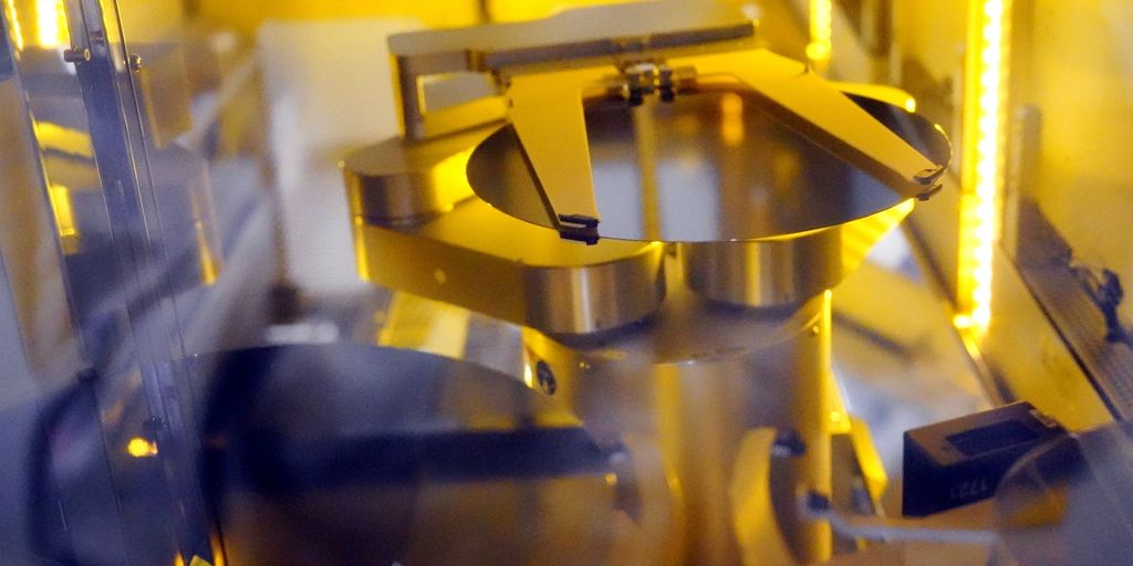
Cutting-Edge Equipment and Tooling
The semiconductor industry is constantly evolving, and cutting-edge advances in equipment and tooling are essential for keeping up with the demand for more advanced electronics. Companies that embrace these innovations position themselves as industry leaders and architects of the technological future.
Emerging Trends in Silicon Wafer Materials
Silicon Carbide (SiC) Wafers
One of the most exciting trends in wafer manufacturing is the use of silicon carbide (SiC) wafers. These wafers are known for their ability to handle high power and high temperatures, making them ideal for power electronics and high-frequency devices. The integration of SiC with traditional silicon wafers opens up new possibilities for advanced device design and performance.
Gallium Nitride (GaN) Wafers
Gallium nitride (GaN) wafers are another significant development. GaN offers unique properties such as high electron mobility and thermal conductivity. These features make GaN wafers suitable for applications in high-power and high-frequency devices. The use of GaN is expanding the horizons of what can be achieved in semiconductor technology.
Alternative Substrates
Beyond SiC and GaN, the exploration of alternative materials is gaining momentum. These materials promise to unlock new capabilities and enhance the performance of electronic devices. As the industry continues to innovate, the use of alternative substrates is expected to play a crucial role in the future of wafer manufacturing.
3D Integration and Through-Silicon Vias (TSVs)
Traditional 2D integration methods are hitting their limits in terms of scalability and performance. Manufacturers are now turning to 3D integration techniques, which involve stacking multiple layers of wafers and connecting them through TSVs. This method allows for higher circuit density, better performance, and shorter interconnect lengths, making it ideal for advanced applications like high-performance computing and artificial intelligence.
Future Directions in Wafer Manufacturing
Research and Development Focus
The journey towards ultra-thin silicon wafer manufacturing continues to evolve. Ongoing research focuses on further improving thickness control, uniformity, and defect reduction. Advancements in thin film transfer technologies and exploration of alternative substrates hold promise for future advancements.
Collaborative Efforts in the Industry
To meet the demands of the rapidly evolving technological landscape, silicon wafer manufacturers are actively investing in research and development to drive innovation. Collaborative efforts among industry leaders, academic institutions, and government agencies are crucial for pushing the boundaries of what’s possible in wafer manufacturing.
Standardization and Quality Control
Standardization and quality control are essential for ensuring the reliability and performance of silicon wafers. As manufacturers embrace cutting-edge technologies and explore novel approaches, the future of silicon wafer manufacturing holds immense promise, shaping the digital landscape for generations to come.
Conclusion
In conclusion, the field of wafer manufacturing has seen remarkable progress through various innovative techniques and technologies. From advanced wafer thinning methods to the development of ultra-thin silicon wafers, each step forward has brought new possibilities for the semiconductor industry. The continuous pursuit of precision and quality has led to the creation of more efficient and reliable electronic devices. As research and development efforts continue, we can expect even more groundbreaking advancements that will shape the future of technology. The journey of innovation in wafer manufacturing is far from over, and the future holds exciting potential for further growth and discovery.
Frequently Asked Questions
What is epitaxy in wafer manufacturing?
Epitaxy is a process where crystalline layers are added to a wafer’s surface. This helps create complex structures with better properties.
How does Chemical Mechanical Planarization (CMP) work?
CMP is a technique that smooths the wafer surface using chemicals and mechanical forces to achieve a flat and even surface.
What are the main steps in wafer thinning?
Wafer thinning usually involves grinding, etching, and polishing to make the wafer thinner with precise control.
What is the importance of silicon carbide (SiC) wafers?
Silicon carbide wafers are important because they offer better performance for power electronics and other special uses.
Why is 3D integration important in wafer manufacturing?
3D integration allows stacking of wafers, which saves space and can improve performance in electronic devices.
What are Through-Silicon Vias (TSVs)?
TSVs are tiny holes that go through a wafer, allowing different layers to connect and communicate, which is key for 3D integration.