Exploring the Critical Role of the Semiconductor Wafer in Modern Technology
Exploring the critical role of the semiconductor wafer in modern technology reveals its foundational impact across various industries. From electronics to space exploration, semiconductor wafers are key to the development and functionality of numerous devices and systems. This article delves into the intricate processes of wafer manufacturing, inspection, and the future prospects of this vital technology.
Key Takeaways
- Semiconductor wafers form the backbone of integrated circuits, essential for modern electronic devices.
- Inspection stages are crucial for ensuring the quality and reliability of semiconductor wafers.
- Photolithography is a pivotal process in wafer manufacturing, affecting the overall quality of semiconductors.
- Semiconductor wafers are integral to advancements in space technology and exploration.
- Future trends in semiconductor wafer technology promise further innovations and enhancements in electronics and beyond.
Understanding Semiconductor Wafer Technology
Fundamentals of Semiconductors
Semiconductors are materials with electrical properties between conductors and insulators. They are typically made from silicon, which is derived from sand. Semiconductors form the basis of modern electronics by allowing the control of electrical currents.
Silicon Wafer Manufacturing Processes
The manufacturing of silicon wafers involves several key steps: crystal growth, wafer slicing, polishing, and cleaning. These processes ensure that the wafers have the necessary quality and surface smoothness for further fabrication.
Advancements in Wafer Technology
Recent advancements in wafer technology include improvements in material quality and the development of larger wafer sizes. These innovations enhance the efficiency of semiconductor devices and allow for more circuits per wafer, reducing costs and improving performance.
The Role of Wafer Inspection in Semiconductor Manufacturing
Importance in Quality Assurance
Wafer inspection is a fundamental aspect of the semiconductor manufacturing process, vitally important for ensuring product quality, improving cost efficiency, and maintaining compliance with industry standards. As technological advancements continue, the role of wafer inspection becomes increasingly vital in producing reliable, high-quality semiconductors.
Stages of Wafer Inspection
Wafer inspection is typically performed at multiple stages throughout the semiconductor manufacturing process, especially after critical steps like photolithography, etching, and doping, to ensure continuous quality control. The following are key stages where wafer inspection is crucial:
- Post-photolithography
- Post-etching
- After doping
Technological Advancements in Inspection
Wafer inspection employs several advanced techniques to identify defects, such as particles, scratches, and pattern irregularities, that can impact device performance and yield. Key techniques include:
- Optical inspection: Involves the use of high-resolution imaging systems and specialized software to identify defects on the wafer surface.
- Other advanced methods: Employ additional technologies to enhance defect detection capabilities and improve overall inspection accuracy.
Photolithography: A Critical Step in Wafer Processing
Photolithography plays a pivotal role in the semiconductor manufacturing process, enabling the precise transfer of complex patterns onto the silicon wafer. This section delves into the intricacies of this essential technique.
Pattern Transfer and Alignment
Photolithography is a crucial optical process in the fabrication process, as it is used to create intricate circuit patterns on a single wafer’s surface. This is achieved by coating the wafer with a photosensitive material, called a photoresist, and then exposing it to high-wavelength deep ultraviolet (DUV) or extreme ultraviolet (EUV) light through a mask containing the desired pattern. The exposed photoresist undergoes a chemical change, which allows it to be selectively removed, leaving behind a precise replication of the pattern.
Challenges in Photolithography
One of the most critical challenges in photolithography is maintaining the alignment of the photomask to the wafer during exposure. Misalignment can lead to defects in the circuit patterns, which can significantly impact the performance of the final semiconductor device. Additionally, the increasing complexity of patterns and the need for smaller feature sizes demand advancements in both photomask technology and exposure systems.
Impact on Semiconductor Quality
The quality of the semiconductor devices heavily relies on the precision of the photolithography process. Any discrepancies in pattern transfer can lead to significant variations in device performance and yield. As such, continuous improvements in photolithography techniques are essential to meet the stringent quality standards required in modern electronics.
The Impact of Semiconductor Wafers on Modern Electronics
Foundation for Microchips
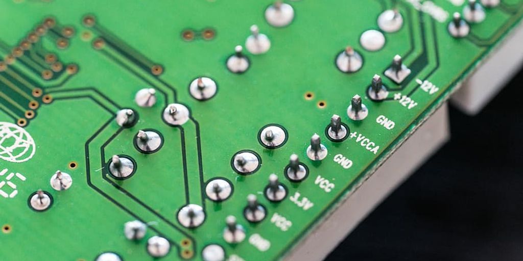
Semiconductor wafers form the essential base for the integrated circuits (ICs) that power virtually all modern electronic devices. From smartphones to computers, the role of these wafers is foundational in the creation of microchips. The process involves multiple complex steps such as cleaning, doping, and etching, which are crucial for the precise functionality of electronic components.
Role in Gaming Consoles
Silicon wafers are pivotal in the development of gaming consoles such as PlayStation 5, Xbox, and Nintendo Switch. These consoles rely on advanced microchips, which are built on these semiconductor wafers, to deliver high-performance gaming experiences. The intricate circuitry that drives these devices originates from the meticulously engineered wafers.
Future Trends in Electronic Devices
Looking ahead, the semiconductor wafer technology is expected to evolve with trends like miniaturization and improved energy efficiency. Innovations such as 3D stacking and wafer-level packaging are set to transform the landscape of electronic devices, making them more powerful yet compact. This evolution will likely continue to drive the capabilities and functionalities of future electronic devices, maintaining the critical role of semiconductor wafers in technology advancement.
Semiconductors and Space Exploration
Contribution to Space Technology
Semiconductors have revolutionized space technology by enabling the miniaturization of electronic components. This transformation allows spacecraft to be smaller, lighter, and more efficient, which is crucial for deep space missions. Semiconductors are integral to the operation of satellites and other spacecraft, providing the necessary computing power and reliability needed in the harsh conditions of space.
Miniaturization of Components
The trend towards smaller and more efficient components has been pivotal in space exploration. Semiconductors enable significant advancements in the design and functionality of space equipment, allowing for sophisticated electronics to be packed into compact spaces. This miniaturization supports the development of new technologies and missions, making space exploration more accessible and less costly.
Future Prospects in Space Exploration
As technology continues to advance, semiconductors will play an increasingly vital role in space exploration. The ongoing development of semiconductor technology promises to enhance the capabilities of spacecraft, enabling more ambitious missions and the potential for new discoveries. The future of space exploration looks promising, with semiconductors at the forefront of this exciting frontier.
Silicon Wafer Packaging and Its Importance
Protection from Environmental Factors
Silicon wafer packaging plays a pivotal role in safeguarding the delicate semiconductor wafers from environmental hazards such as chemical contamination, physical damage, and adverse weather conditions. This protective measure is essential for maintaining the integrity and functionality of the wafers throughout their lifecycle.
Types of Wafer Packaging
Various materials are used for wafer packaging, including metal, plastic, ceramic, and glass. Each type offers different levels of protection and connectivity, influencing the overall performance and durability of the semiconductor device.
Influence on Semiconductor Performance
The choice of packaging material and technique directly impacts the semiconductor’s performance. Advanced packaging is crucial for enhancing the thermal conductivity, minimizing potential warpage, and supporting the miniaturization of integrated circuits, which are vital for the development of compact, high-performance electronic devices.
The Future of Semiconductor Wafer Technology
Innovations on the Horizon
The semiconductor industry’s trajectory is closely tied to technological advancements in many fields of human activity. As we look to the future, innovations such as the use of graphene and other 2-D materials are being explored. These materials promise to overcome the limitations of traditional silicon and potentially revolutionize the performance and functionality of semiconductor devices.
Challenges and Opportunities
Embracing new materials and innovative manufacturing techniques is essential for semiconductor manufacturers to stay competitive. The shift towards advanced packaging, which aggregates components from various wafers into a single device, exemplifies such innovation. This approach not only enhances device performance but also poses significant challenges in manufacturing complexity and cost.
Predictions for the Next Decade
Over the next decade, we can expect the semiconductor industry to continue its rapid evolution. Key trends likely to shape this landscape include sustainability initiatives and the increasing demand for high-performance computing solutions. The future of game consoles and other consumer electronics will heavily rely on further advancements in semiconductor wafer technology, ensuring a vibrant market and continuous innovation.
Conclusion
In the realm of modern technology, semiconductor wafers play an indispensable role, serving as the backbone for the integrated circuits that power our electronic devices. From enhancing gaming experiences on the latest consoles to enabling advancements in space exploration, the importance of these wafers cannot be overstated. As technology progresses, the continuous improvement and rigorous inspection of semiconductor wafers will remain crucial in meeting the growing demands for high-quality, reliable, and efficient electronic devices. The journey of understanding and innovating semiconductor technology is ongoing, and the semiconductor wafer will continue to be at the heart of this evolution, driving the future of technology.
Frequently Asked Questions
What is a semiconductor wafer?
A semiconductor wafer is a thin slice of semiconductor material, such as silicon, used in the fabrication of integrated circuits and other microdevices. It serves as the substrate on which microcircuits are built through various processes like photolithography and etching.
Why is wafer inspection crucial in semiconductor manufacturing?
Wafer inspection is vital to ensure the quality and reliability of semiconductors. It helps identify defects or misalignments in the patterns imprinted on the wafers during photolithography, preventing potential circuit failures.
How does photolithography impact semiconductor quality?
Photolithography is a critical process in semiconductor manufacturing where patterns are transferred onto wafers. Accurate pattern transfer and alignment are essential for high-quality circuitry, impacting the overall performance and reliability of semiconductor devices.
What role do silicon wafers play in modern electronics?
Silicon wafers form the foundation upon which all modern electronic microchips are built. They are crucial for the manufacturing of high-performance integrated circuits found in devices like smartphones, computers, and gaming consoles.
How do advancements in wafer technology benefit space exploration?
Advancements in wafer technology, such as miniaturization and improved performance, play a significant role in space exploration. They enable the development of more compact, efficient, and powerful components essential for space technology and missions.
What are the future trends in semiconductor wafer technology?
Future trends in semiconductor wafer technology include further miniaturization, increased efficiency, and the integration of new materials to enhance performance. These advancements are expected to drive innovation in various fields, including electronics and space exploration.