Exploring the Wafer Manufacturing Process: From Start to Finish
The journey from raw silicon to a polished, tested silicon wafer encapsulates the essence of silicon wafer manufacturing. This process combines advanced technology, precision engineering, and stringent quality control to produce the fundamental building block of the semiconductor industry, enabling the vast array of electronic devices that power our modern world. In this article, we will explore the silicon wafer processing and manufacturing, from raw material acquisition to final wafer characterization and inspection.
Key Takeaways
- Silicon wafers start their journey as raw materials, which are purified and transformed into cylindrical ingots using techniques like the Czochralski process or the Float Zone method.
- The quality of the crystal growth stage is crucial, as it determines the wafer’s performance and reliability in semiconductor applications.
- Wafer slicing and polishing are critical steps to ensure an extremely smooth surface, which is essential for subsequent photolithography and patterning processes.
- Photolithography is a precise process where intricate patterns are created on the wafer’s surface using light exposure and chemical processes.
- Rigorous testing and inspection at various stages ensure that the wafers meet stringent quality standards, making them reliable for high-performance electronic devices.
Raw Material Extraction and Purification
Sources of Silicon
The primary raw material used in silicon wafer manufacturing is silica sand, which is abundant in nature. However, not all sand is suitable for manufacturing high-quality silicon wafers. The sand must be high-purity, with low impurities, such as iron, aluminum, and other materials, to ensure that the resulting silicon wafers are of high quality.
Purification Techniques
To obtain the necessary purity, the sand is washed and dried to remove any impurities affecting the silicon wafers’ quality. It is then subjected to a high-temperature process to convert it into pure silicon. This purified silicon is essential for the subsequent steps in wafer manufacturing.
Formation of Silicon Ingots
Once purified, the silicon is transformed into large cylindrical ingots. These ingots are extracted through a complex process involving techniques like the Czochralski process or the Float Zone method. The resulting ingots are then ready for the next stages of wafer manufacturing.
Crystal Growth Methods
Crystal growth is the process of producing a large, high-quality semiconductor crystal, which serves as the starting material for wafer production. For silicon-based devices, the most common method of crystal growth is the Czochralski process. This method involves melting high-purity silicon in a crucible and cooling it to a temperature near the freezing point. Then the process allows for the formation of a single silicon crystal.
Czochralski Process
The Czochralski process is a widely used method for growing large, single-crystal silicon ingots. It involves the following steps:
- Melting high-purity silicon in a quartz crucible.
- Inserting a seed crystal into the molten silicon.
- Slowly pulling the seed crystal upwards while rotating it, allowing the silicon to solidify in a single-crystal structure.
Float Zone Method
The Float Zone method is another technique particularly useful for producing very high-purity silicon crystals. This method involves passing a rod of polycrystalline silicon through a radio frequency (RF) heating coil, which melts a small region of the rod. The molten zone is then moved along the rod, allowing the silicon to recrystallize with fewer impurities.
Quality Control in Crystal Growth
Quality control is crucial in the crystal growth process to ensure the production of defect-free silicon crystals. Techniques such as X-ray diffraction and infrared spectroscopy are used to detect and measure crystal defects. Additionally, maintaining a controlled environment during the growth process helps minimize contamination and defects.
Wafer Slicing and Polishing
After the silicon ingots have been created, they undergo slicing and polishing to transform them into usable wafers. The ingots are sliced into thin circular disks, with the thickness carefully controlled based on the desired specifications. This process is achieved using advanced cutting techniques, such as wire sawing or diamond blade cutting. Following the slicing, the wafers undergo a polishing stage to remove any imperfections and achieve the required smoothness and flatness.
Photolithography and Patterning
Photolithography is a crucial optical process in the fabrication process, as it is used to create intricate circuit patterns on a single wafer’s surface. This is achieved by coating the wafer with a photosensitive material, called a photoresist, and then exposing it to high-wavelength deep ultraviolet (DUV) or extreme ultraviolet (EUV) light through a mask containing the desired pattern. The exposed photoresist undergoes a chemical change, which allows it to be selectively removed. This leaves behind a precise pattern that is essential for the subsequent steps in semiconductor manufacturing.
Doping and Ion Implantation
Doping and ion implantation are crucial steps in the fabrication process, as they allow for the creation of n-type and p-type semiconductor regions within the device. Doping involves the introduction of impurities, or dopants, into the semiconductor material, which significantly alters its electrical properties. These impurities include the introduction of trivalent or pentavalent impurities. Injection of the diffusion layer, heating semiconductor material, and ion implantation are common methods of introducing dopant atoms.
Introduction of Impurities
Doping involves the introduction of impurities into the semiconductor material. These impurities can be trivalent or pentavalent atoms, which significantly alter the electrical properties of the material. The process is essential for creating n-type and p-type regions within the semiconductor device.
Doping Techniques
Ion implantation is the most common doping technique that involves bombarding the wafer with a beam of ions. The ions are ionized, accelerated using an electric field, and directed toward the wafer surface. The high-energy ions penetrate the wafer and become embedded in the crystal lattice, altering the electrical properties of the material. Ion implantation offers several advantages over other doping techniques, including:
- Precise control over the dopant concentration and depth
- Uniform dopant distribution across the wafer surface
- Low-temperature processing, which reduces the risk of damage to the wafer
However, ion implantation can also cause damage to the crystal lattice, which must be repaired through a subsequent annealing process.
Impact on Semiconductor Properties
The introduction of dopants into the semiconductor material significantly alters its electrical properties. The process allows for the creation of n-type and p-type regions, which are essential for the functionality of semiconductor devices. Although ion implantation is the dominant method of creating selective doping in Si devices, challenges exist in its use for WBG devices. The high-energy ions used in ion implantation can cause damage to the crystal lattice, which must be repaired through annealing. Despite these challenges, ion implantation remains a widely used and effective doping technique in semiconductor manufacturing.
Wafer Testing and Inspection
Wafer testing and inspection are crucial steps in the semiconductor manufacturing process to ensure the quality and reliability of the final product. Rigorous testing identifies and eliminates defective components, ensuring the semiconductor wafers meet quality standards.
Final Wafer Preparation
The final wafer preparation stage is crucial in ensuring the quality and reliability of semiconductor devices. This stage involves several meticulous processes to prepare the wafer for packaging and final quality checks.
Cleaning Processes
The silicon wafers are subjected to chemical and mechanical cleaning processes to remove residual impurities and prepare the surface for further processing. These cleaning steps are essential to ensure that the wafers are free from contaminants that could affect the performance of the semiconductor devices.
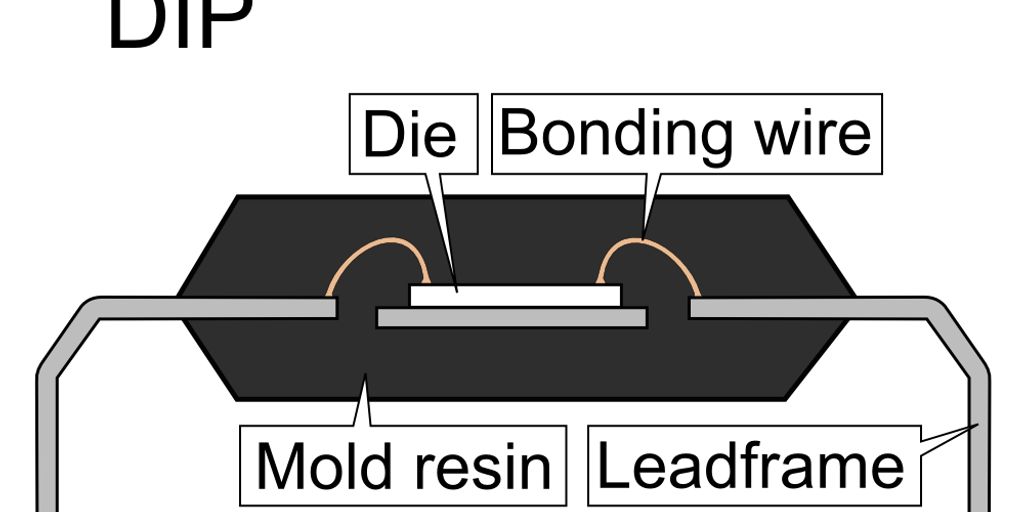
Packaging Methods
Once the wafers are thoroughly cleaned, they are ready for packaging. Packaging methods vary depending on the type of semiconductor device being produced. The goal is to protect the wafer from physical damage and contamination during handling and transportation. Proper packaging is vital to maintain the integrity of the wafers until they reach their final destination.
Final Quality Checks
Before the wafers are shipped out, they undergo final quality checks to ensure they meet all specifications. These checks include visual inspections, electrical testing, and other quality assurance protocols. Only wafers that pass these stringent tests are approved for use in semiconductor manufacturing.
Conclusion
This journey from a single crystal to a polished, tested silicon wafer encapsulates the essence of silicon wafer manufacturing. It’s a process that combines advanced technology, precision engineering, and stringent quality control to produce the fundamental building block of the semiconductor industry, enabling the vast array of electronic devices that power our modern world. By carefully controlling each step—from raw material extraction and purification to wafer slicing, polishing, and final inspection—manufacturers ensure the production of high-quality wafers that meet the stringent requirements necessary for reliable, high-performance semiconductor devices. The wafer manufacturing process is not just about creating a product; it is about laying the foundation for the future of technology.
Frequently Asked Questions
What are silicon wafers?
Silicon wafers are thin slices of semiconductor material, typically silicon, used in the fabrication of integrated circuits and other microdevices. They serve as the substrate for microelectronic devices.
Why is the silicon wafer manufacturing process important?
The silicon wafer manufacturing process is crucial because it directly affects the performance and reliability of electronic devices. Each step, from raw material extraction to final inspection, ensures the wafers meet stringent quality standards.
What is the Czochralski process?
The Czochralski process is a method of crystal growth used to obtain single crystals of semiconductors like silicon. It involves melting high-purity silicon and then slowly pulling a seed crystal from the melt, forming a cylindrical ingot.
How are silicon wafers sliced and polished?
Silicon wafers are sliced from cylindrical ingots using precision saws. The sliced wafers are then polished using chemical and mechanical processes to achieve an extremely smooth surface, essential for subsequent photolithography and patterning.
What role does photolithography play in wafer manufacturing?
Photolithography is a process used to transfer intricate circuit patterns onto the silicon wafer. It involves creating a photomask, exposing the wafer to light, and developing the exposed areas to form the desired patterns.
How are defects detected in silicon wafers?
Defects in silicon wafers are detected using various inspection and testing methods, including visual inspection, electrical testing, and advanced imaging techniques. These methods ensure that wafers meet quality standards before proceeding to the next manufacturing stage.