From Silicon to Chip: A Step-by-Step Guide to the Semiconductor Manufacturing Process
The creation of semiconductors is a marvel of modern engineering, transforming ordinary sand into the complex chips that power our world. This intricate process spans from the meticulous crafting of silicon wafers to the sophisticated design and assembly of integrated circuits. In this article, we’ll navigate through each pivotal step of semiconductor manufacturing, unveiling the precision and innovation behind the chips that drive today’s technology.
Key Takeaways
- The semiconductor manufacturing process is a complex journey from sand to sophisticated chips, involving precise control over multiple steps.
- Silicon wafers are the foundation of semiconductors, created through the Czochralski method and meticulous slicing, etching, and polishing.
- Integrated circuit design is a critical phase where functionality is translated into circuit patterns, requiring thorough simulation and verification.
- Front-end and back-end processing encompass a series of sub-processes like oxidation, photolithography, and 2.xD/3D packaging to craft and assemble the chip.
- Innovations such as AutoML systems and sustainability practices are shaping the future of semiconductor manufacturing, aiming to push performance limits while addressing scalability challenges.
Silicon Wafer Manufacturing: The Foundation of Semiconductors
The Journey from Sand to Silicon
The transformation of humble sand into the foundational material for semiconductors is a marvel of modern engineering. Silicon, the second most abundant element on Earth, begins its journey as silica sand. This sand is subjected to high temperatures, melting it into a pure form. A seed crystal of silicon is then introduced into the molten sand, initiating the growth of a silicon ingot through a process known as the Czochralski method.
Once the ingot is formed, precision is key in the next steps. The ingot is sliced into wafers using a diamond saw, ensuring each wafer is of the necessary thinness and flatness for subsequent manufacturing processes. These wafers are then meticulously etched and polished, resulting in a surface that must meet exacting standards of smoothness and uniformity. This meticulous preparation is crucial as it sets the stage for the intricate patterns of an integrated circuit to be imprinted upon them.
The following list outlines the key stages in the journey from sand to silicon:
- Heating silica sand beyond its melting point
- Introducing a silicon seed crystal
- Growing a silicon ingot using the Czochralski method
- Slicing the ingot into wafers with a diamond saw
- Etching and polishing wafers to achieve a smooth surface
The Czochralski Method and Ingot Formation
The Czochralski method is a pivotal step in semiconductor manufacturing, where a single crystal of silicon is grown from molten silicon. The process begins with the melting of high-purity silica sand, which is then carefully controlled to maintain a stable temperature just above its melting point. A precisely oriented seed crystal is dipped into the molten silicon, and as it’s slowly withdrawn, a cylindrical ingot of single-crystal silicon forms around it. This ingot is the precursor to the silicon wafers that are fundamental to all semiconductor devices.
Once the ingot has been formed, it undergoes a series of processes to transform it into usable wafers. The ingot is first mounted on a specialized holder and then sliced into thin discs using a high-precision diamond saw. These slices, or wafers, are then polished to create a mirror-like surface that is essential for the subsequent layers of semiconductor fabrication. The entire process is meticulously monitored to ensure the highest quality and uniformity of the wafers.
Slicing and Polishing: Preparing the Wafer
Once the solid silicon ingot is formed, it is sliced into thin wafers using a diamond saw. This step is crucial as it guarantees the wafers’ optimal thinness and flatness, which are essential for the subsequent manufacturing processes. The slicing process, however, can introduce microscopic defects to the wafer surface, affecting the crystal structure.
After slicing, the wafers are subjected to a series of etching and polishing steps. The goal is to achieve a surface that is as smooth and uniform as possible. This is critical for precision processing and testing, ensuring that the wafers meet the stringent standards required for semiconductor manufacturing. The etching process helps to remove any damaged layers or contaminants from the wafer surface, while polishing refines the surface to an atomic level of smoothness.
The final quality of the wafer surface is paramount, as any imperfections can lead to defects in the semiconductor devices later on. Therefore, each wafer is rigorously inspected and tested to ensure it meets the necessary specifications before moving on to the next phase of manufacturing.
Integrated Circuit Design: Blueprinting the Chip
Translating Functionality into Circuit Patterns
The intricate process of translating functionality into circuit patterns is a pivotal step in semiconductor chip design. It involves the meticulous conversion of the chip’s intended functions into a detailed blueprint that will guide the subsequent manufacturing stages. This blueprint is known as the architectural layout, which maps billions of transistors and electronic components to relay instructions to the device’s software.
The architectural design is translated into a Register-Transfer Level (RTL) description, specifying the data flow and control elements of the chip’s functionality. This RTL description serves as a cornerstone for the chip’s design, ensuring that the final product will perform as intended within its operating environment. The following list outlines the key roles in this process:
- Fabless: A semiconductor design company that may outsource wafer fabrication.
- Chip design: The R&D-intensive task of creating the chip’s architecture.
- Foundry: A manufacturing facility for semiconductor chips, often used by companies without their own wafer fabrication capabilities.
- Integrated Device Manufacturer (IDM): A company that handles design, manufacturing, and sales of ICs.
Simulation and Verification of Design
Once the integrated circuit design is finalized, it undergoes a critical phase of simulation and verification. This process ensures that the chip will function correctly within its intended operating environments. It’s a meticulous step that tests the integrated circuit within its package for functionality, performance, and compliance with specified standards.
Reliability testing is a cornerstone of this phase, involving the wafers being subjected to various stress conditions to predict their lifespan and performance under different scenarios. This practice is crucial for guaranteeing that the semiconductors will perform reliably in real-world conditions.
The integration of simulation and verification with the manufacturing workflow is essential for process control and optimization. Regular monitoring and fine-tuning of the process parameters are conducted to maintain high standards of quality and efficiency. Strategies like Statistical Process Control (SPC) provide a systematic approach to process monitoring, which is integral to the semiconductor manufacturing process.
Preparing for the Front-End Process
With the integrated circuit design finalized, the semiconductor manufacturing process is poised to enter the front-end-of-the-line (FEOL) phase. This critical juncture involves transforming the abstract design into a physical reality on the silicon wafer. To ensure a seamless transition, several preparatory steps are undertaken:
- Material selection: Choosing the appropriate materials that will form the various layers and structures of the chip.
- Equipment calibration: Fine-tuning the sophisticated machinery for processes like photolithography and etching.
- Process optimization: Adjusting parameters to achieve the best possible fidelity between the design and the manufactured chip.
These preparations are essential for the intricate work of creating transistors and other microscopic structures that define the chip’s functionality. The FEOL stage is where the foundation for the chip’s performance and capabilities is laid, making the preparatory work crucial for the success of the entire semiconductor manufacturing process.
Front-End Processing: Crafting the Semiconductor
Oxidation and Photolithography: Patterning the Silicon
The front-end process is where the actual circuitry of a semiconductor is formed. Oxidation is one of the initial steps, where the silicon wafer is exposed to oxygen or steam at high temperatures to grow a layer of silicon dioxide on its surface. This layer serves multiple purposes, including acting as a barrier during subsequent doping processes and as a dielectric material in the final device.
Photolithography follows oxidation and is a pivotal technique in defining the intricate patterns of the integrated circuit. In this process, a light-sensitive chemical called a photoresist is applied to the wafer. Then, using a photomask that blocks light in certain areas, ultraviolet light is shone onto the wafer. The exposed areas of the photoresist harden, while the unexposed areas are washed away, leaving behind a pattern that mirrors the photomask. This patterned photoresist then guides the etching process that carves the desired structures into the silicon.
The precision and complexity of photolithography have made it a cornerstone of semiconductor manufacturing. The process has evolved to include multiple steps of coating, exposure, and development to achieve the necessary resolution for today’s high-performance chips. Here is a simplified list of the photolithography steps:
- Apply photoresist coating to the wafer
- Prebake to remove solvents
- Expose to ultraviolet light through a photomask
- Post-exposure bake to further harden the photoresist
- Develop the photoresist to reveal the pattern
- Inspect and prepare for etching
Etching and Cleaning: Defining the Structures
After the intricate patterns are defined on the silicon wafer through photolithography, the etching process takes center stage. This critical step involves selectively removing material to create the desired structures on the chip. Various etching techniques are employed, each suited to different materials and design requirements. For instance, wet etching uses chemical solutions to dissolve unwanted material, while dry etching involves gases that react with the surface to be etched, often under vacuum conditions.
The cleaning process follows etching to ensure that any residual particles or chemicals are removed. This step is essential to maintain the integrity of the semiconductor structures. Cleaning methods range from simple rinsing with deionized water to more complex procedures involving ultrasonic baths or high-pressure jets. The goal is to achieve a wafer surface that is impeccably clean and free from contaminants, which could otherwise lead to defects in the final product.
Here is a brief overview of common etching techniques used in semiconductor manufacturing:
- Wet Etching: Involves chemical solutions for material removal.
- Dry Etching: Employs reactive gases, often in a plasma state.
- Reactive Ion Etching (RIE): A type of dry etching that uses ions to remove material.
- Deep Reactive Ion Etching (DRIE): Suitable for creating deep, vertical structures.
Each technique has its own set of parameters that must be meticulously controlled to achieve the desired outcome. The choice of etching method depends on factors such as the type of material, the level of precision required, and the specific design of the semiconductor device.
Doping and Planarization: Modifying Electrical Properties
The semiconductor manufacturing process is a marvel of modern engineering, involving a series of intricate steps to transform a simple silicon wafer into a complex integrated circuit. Doping and planarization are critical stages that modify the electrical properties of the silicon to create the desired semiconductor devices.
Doping involves introducing specific impurities into the silicon substrate to alter its conductivity. This is achieved through various techniques such as ion implantation or diffusion. The choice of dopant and the level of concentration determine the type of charge carrier (electron or hole) and the conductivity of the semiconductor.
Planarization, on the other hand, is the process of smoothing the wafer surface to ensure uniformity and flatness. This is essential for the subsequent photolithography steps, where an even surface is crucial for pattern precision. Chemical Mechanical Planarization (CMP) is a common method used to achieve the desired surface quality.
The table below summarizes the key aspects of these processes:
| Process | Purpose | Technique |
|---|---|---|
| Doping | Alter conductivity | Ion implantation, Diffusion |
| Planarization | Smooth surface | Chemical Mechanical Planarization (CMP) |
As we advance through the semiconductor manufacturing process, these modifications lay the groundwork for the intricate circuit patterns that will soon be etched into the silicon, bringing us one step closer to the final product.
Back-End Processing: From Silicon to System
Mounting and Interconnection: Assembling the Chip
Once the functional dies are packaged, they are placed in a protective casing, marking a critical phase in semiconductor device fabrication. This casing not only safeguards the delicate die but also provides the necessary external contacts for subsequent integration into electronic systems. The process encompasses several meticulous sub-steps, such as die attachment, wire bonding or flip-chip bonding, and encapsulation. These steps are pivotal in ensuring that the die is securely positioned and electrically connected within its package.
The encapsulation serves a dual purpose: it shields the die from environmental hazards and mechanical damage, and it facilitates the die’s mounting on a circuit board. Post-packaging, the chips are subjected to rigorous final testing to verify their functionality and performance. This testing phase is crucial to ensure that the integrated circuit operates correctly within its intended operating environments and adheres to the specified standards.
The advent of advanced packaging technologies, such as 2.xD and 3D, has significantly enhanced the density and performance of chip mounting in the back-end process. These innovative approaches allow for a more efficient use of space and improved electrical properties, which are essential for the development of high-performance chips.
2.xD and 3D Packaging Technologies
The evolution of high-performance semiconductor chips has been pushing the boundaries of what’s possible in the front-end manufacturing process. However, as these advancements approach their physical and economic limits, the industry has turned its focus to the back-end process, where 2.xD and 3D packaging technologies have emerged as pivotal innovations. These technologies are not just buzzwords; they represent a significant leap in the way semiconductor chips are assembled and interconnected.
2.xD and 3D packaging solutions enable high-density mounting of semiconductor chips, which is crucial for the miniaturization and performance enhancement of electronic devices. By stacking chips vertically or placing them on an interposer, these packaging methods allow for more components to be packed into a smaller footprint. This is particularly important for applications where space is at a premium, such as in mobile devices and wearables.
The impact of these packaging technologies extends beyond just physical dimensions. They also contribute to improved electrical performance and heat dissipation, which are critical for maintaining the reliability and efficiency of semiconductor devices. As the industry continues to innovate, companies like Resonac are at the forefront, driving research and development through initiatives like the Packaging Solution Center and the JOINT2 consortium. These collaborative efforts are essential for advancing packaging materials and techniques that will support the next generation of semiconductor technology.
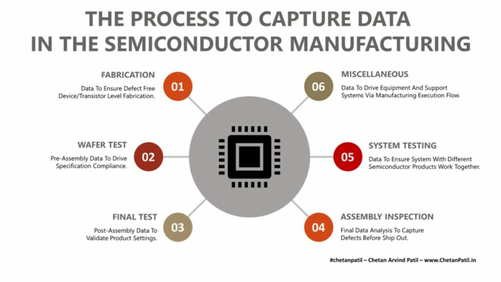
Testing and Quality Assurance: Ensuring Reliability
Ensuring the long-term reliability of semiconductor devices is a critical aspect of the manufacturing process. Reliability testing is a rigorous phase where wafers are subjected to various stress conditions to predict their lifespan and performance in different scenarios. This step is crucial for confirming that the chips will function reliably under real-world conditions.
Quality control is maintained through routine inspections and regular calibration of testing equipment, such as wafer probers and probe stations. These tools are essential for accurately assessing each wafer’s performance. Effective data analysis is also vital, as it allows for the identification of issues and trends, and troubleshooting skills are necessary to resolve any problems that arise.
The integration of testing into the manufacturing workflow involves a continuous process of control and optimization. Regular monitoring and fine-tuning of process parameters are essential to maintain high standards of quality and efficiency. Techniques like Statistical Process Control (SPC) offer a systematic approach to ensuring that every chip meets the stringent requirements set forth by the industry.
| Process Step | Tool Used | Purpose |
|---|---|---|
| Inspections | Various | Ensure equipment accuracy |
| Wafer Probing | Wafer Probers | Assess wafer performance |
| Data Analysis | Analytical Software | Identify issues and trends |
| Process Control | SPC Techniques | Maintain quality and efficiency |
Innovations and Challenges in Semiconductor Manufacturing
Pushing the Limits: Evolution of High-Performance Chips
The relentless pursuit of higher performance in semiconductor chips is approaching a critical threshold where traditional front-end improvements are yielding diminishing returns. Innovations in 2.xD and 3D packaging technologies have emerged as pivotal in enabling manufacturers to achieve high-density chip integration and enhanced performance in the back-end process.
Intel’s recent strategic moves underscore the industry’s shift towards self-reliance and diversification of manufacturing capabilities, particularly in response to geopolitical uncertainties affecting chip supply chains. This is part of a broader trend where companies are investing heavily in domestic production to secure a stable supply of the advanced chips necessary for AI and accelerated computing.
Challenges persist, as illustrated by NI’s experiences with wafer and chip processing defects. These issues underscore the complexity of semiconductor manufacturing and the need for continuous innovation to maintain high yields of functional devices. The table below highlights the key areas of focus for future advancements in high-performance chip manufacturing:
| Focus Area | Description |
|---|---|
| Packaging Technologies | Advancements in 2.xD and 3D integration for higher density and performance. |
| Domestic Production | Investment in local manufacturing to mitigate supply chain risks. |
| Yield Improvement | Research into defect reduction and process optimization for better yields. |
Smart Manufacturing and AutoML Systems
The integration of AutoML systems into semiconductor manufacturing heralds a new era of efficiency and precision. AutoML stands to revolutionize the industry by automating the optimization of production processes, enhancing quality control, and enabling predictive maintenance. By leveraging adaptive modeling, these systems can recommend optimal solutions for defect classification and algorithm selection, aiding experts in pinpointing production bottlenecks.
Despite the promise of AutoML, its deployment faces significant challenges. Current general-purpose AutoML models lack the specialized response capabilities needed for the semiconductor industry’s unique issues. Moreover, the end-to-end ‘black box’ nature of these systems can obscure the logic behind their decisions, complicating their integration into highly complex manufacturing processes.
To address these challenges, recent advancements propose a domain-specific AutoML framework designed to:
- Enhance yield rates with more accurate and efficient performance.
- Integrate explainable methods for a transparent and reliable AutoML pipeline.
- Foster self-adaptation, self-optimization, and automation within smart manufacturing solutions.
This tailored approach aims to not only improve the yield but also to make the AutoML process more understandable and trustworthy for industry professionals.
Future Trends: Sustainability and Scalability
The semiconductor industry is on the brink of a transformative era, where sustainability and scalability are becoming paramount. As the demand for semiconductors skyrockets, largely driven by the surge in use for generative AI, the industry faces the challenge of innovating faster and producing more capable and efficient chips. This necessitates a shift towards more sustainable manufacturing practices and the development of scalable solutions that can meet the growing needs without compromising on environmental responsibilities.
To address these challenges, the industry is exploring various avenues. One such approach is the integration of smart manufacturing systems that leverage artificial intelligence to optimize operations. These systems aim to transform the traditional manufacturing pyramid into an advanced, autonomous intelligent system with cognitive decision-making capabilities. However, the deployment of such ML techniques often requires extensive expertise, which presents a barrier to rapid integration.
The future of semiconductor manufacturing will likely involve a combination of advanced ML algorithms, generative AI, and other innovative technologies to create a responsive and efficient manufacturing ecosystem. This will not only improve product yields and optimize resource utilization but also ensure that the industry can adaptively optimize manufacturing to realize smart, sustainable manufacturing (SSM).
Conclusion
In this comprehensive guide, we have journeyed through the intricate and precise world of semiconductor manufacturing, from the initial silicon wafer production to the advanced packaging technologies that define modern chips. We’ve seen how the process is a symphony of complex steps, each requiring meticulous control and understanding. The evolution of semiconductor technology continues to push the boundaries of innovation, with 2.xD and 3D packaging emerging as pivotal in enhancing chip performance. As the industry confronts the challenges of scaling and complexity, the insights and best practices discussed here are invaluable for professionals striving to maintain quality and efficiency in semiconductor production. The future of this field is undoubtedly bright, with ongoing advancements promising to further revolutionize our technological landscape.
Frequently Asked Questions
What are the four major links in the semiconductor manufacturing process?
The four major links in the semiconductor manufacturing process are silicon wafer manufacturing, integrated circuit design, front-end process, and back-end process.
Why is wafer testing critical in the semiconductor industry?
Wafer testing is critical because it ensures that each wafer meets the required standards for quality and performance, which is essential for the reliability of semiconductor devices.
What is AutoML and how does it relate to semiconductor manufacturing?
AutoML stands for Automated Machine Learning, and in semiconductor manufacturing, it refers to smart systems that can provide explanations for model outputs, help map inputs to outputs, and identify causes of low yield.
What are the challenges faced in semiconductor manufacturing?
Semiconductor manufacturing faces challenges such as the complexity of the process, the need for precise control over numerous steps, and the continuous push for technological and cost performance improvements.
How are 2.xD and 3D packaging technologies impacting semiconductor manufacturing?
2.xD and 3D packaging technologies are becoming key in manufacturing high-performance semiconductor chips, allowing for high-density mounting and improved chip performance.
What is the Czochralski method and how is it used in wafer manufacturing?
The Czochralski method is a technique used to grow single crystal silicon ingots by inserting a seed crystal into molten silica sand. The resulting ingot is then sliced into wafers for semiconductor manufacturing.