Harnessing the Power of Silicon Carbide: Breakthroughs in Wafer SiC Technology
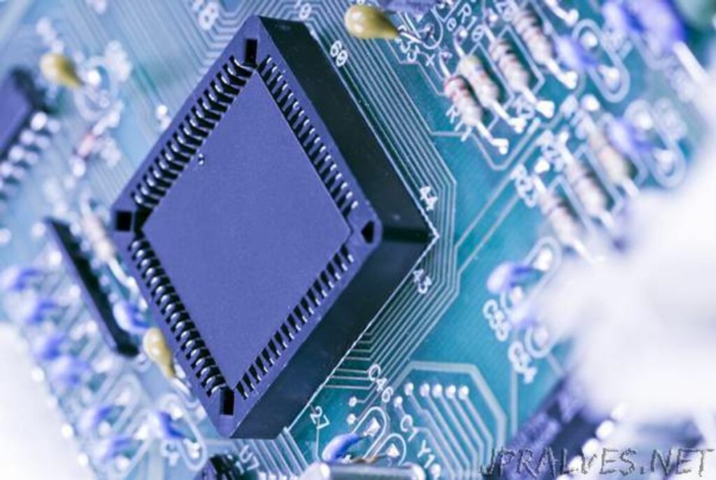
Silicon carbide (SiC) technology is revolutionizing the semiconductor industry with its superior properties over traditional silicon. This article delves into the latest breakthroughs in SiC wafer technology, exploring how advancements in substrate quality, manufacturing techniques, and innovative applications are driving performance and reliability in power devices. We’ll also examine SiC’s pivotal role in automotive electronics, compare it with other wide-bandgap semiconductors, and discuss the future of SiC in various high-tech fields.
Key Takeaways
- Enhanced SiC substrate quality and manufacturing innovations are pivotal for the next generation of high-performance power devices, offering improved efficiency and reliability.
- SiC technology is becoming a cornerstone in automotive electronics, providing significant advantages in electric vehicles and charging infrastructure due to its efficiency and thermal management capabilities.
- Comparative studies of wide-bandgap semiconductors reveal SiC’s competitive edge over GaN in certain power electronics applications, highlighting the importance of substrate material choices.
- The reliability and lifetime of SiC devices are being extended through advanced assessment techniques and predictive maintenance, ensuring long-term stability in demanding applications.
- Emerging applications of SiC, including renewable energy systems, quantum computing, and medical equipment, showcase the material’s versatility and potential to transform various industries.
Advancements in SiC Substrate Technology
Improving Substrate Quality for Enhanced Device Performance
The relentless pursuit of performance in silicon carbide (SiC)-based power devices has placed a spotlight on the quality of SiC substrates. Advancements in substrate quality are pivotal for achieving reduced defect densities and enhanced reliability in these devices. Researchers are focused on identifying and eliminating critical defects that impede device efficiency. The quest for perfection in substrate quality is not just about reducing defects; it also encompasses improving the mechanical properties of wafers, such as flatness and uniformity in thickness.
Efforts to refine substrate quality involve a multi-faceted approach:
- Defect Density Reduction: Targeting specific defects that critically affect device performance.
- Mechanical Property Enhancement: Ensuring wafers exhibit silicon-like flatness and minimal local thickness variations.
- Economic and Sustainable Manufacturing: Developing methods like Atomic Layer Etching (ALE) that are cost-effective and produce fewer unsustainable by-products.
These improvements are not merely incremental; they are essential for the next generation of SiC power devices that will demand even greater performance and reliability. As the material quality progresses, the industry anticipates a significant impact on a wide array of applications, from mobile phones to medical devices, reducing electronic waste through increased device longevity.
Innovations in Manufacturing Techniques
The evolution of manufacturing techniques for silicon carbide (SiC) wafers has been pivotal in meeting the growing demand for high-performance semiconductors. Innovative approaches have streamlined the production process, enhancing throughput and reducing costs. One such advancement is the refinement of Chemical Mechanical Planarization (CMP), a critical step in wafer production.
Recent developments have focused on reducing the CMP polishing time, which has traditionally been a bottleneck in SiC wafer fabrication. Hyperion’s novel solution exemplifies this progress, significantly boosting SiC production by optimizing the final CMP stage. This improvement not only accelerates production but also contributes to the overall substrate quality, which is essential for the next generation of electronic devices.
The table below summarizes the impact of these innovations on SiC wafer production:
| Technique | Benefit | Result |
|---|---|---|
| Advanced CMP | Reduced polishing time | Increased throughput |
| Precision Machining | Enhanced substrate quality | Improved device performance |
| Additive Manufacturing | Customization capability | Bespoke device fabrication |
As the industry continues to evolve, these manufacturing innovations lay the groundwork for a future where SiC technology can be tailored to specific applications, ensuring optimal performance across various sectors.
Optimizing Substrate Properties for Future Applications
The relentless pursuit of efficiency in power devices has led to significant advancements in substrate technology, particularly for silicon carbide (SiC). Researchers are continuously working to enhance the properties of SiC substrates to meet the evolving demands of various applications. The choice of substrate material is crucial, impacting not only device performance but also reliability and manufacturability.
To address these challenges, a multi-faceted approach is being adopted. Innovations in manufacturing techniques have led to improved substrate quality, which in turn reduces defects and enhances device reliability. Moreover, there is a growing emphasis on application-specific optimization of SiC technologies. For instance, the requirements for automotive applications may differ from those for industrial or medical equipment, necessitating tailored substrate properties.
The table below summarizes the key areas of focus for optimizing SiC substrate properties:
| Area of Focus | Description |
|---|---|
| Quality Improvement | Enhancing crystal purity and reducing micro-defects |
| Manufacturing Innovations | Developing cost-effective and scalable production methods |
| Application-Specific Design | Tailoring substrates to specific end-use requirements |
As we move forward, the integration of advanced computational tools, such as the Schrödinger software, is expected to play a pivotal role in refining the etch rates and consistency of SiC substrates. This will not only improve the performance of existing devices but also pave the way for new applications, reducing the environmental impact by increasing the longevity of semiconductor-based products.
Silicon Carbide in Automotive Electronics
Efficiency and Reliability in Power Devices
Silicon carbide (SiC) power devices are increasingly becoming the cornerstone of power electronics due to their superior properties. SiC power devices offer a multitude of advantages over conventional silicon-based devices, such as higher breakdown voltage and lower on-state resistance, which translate into improved efficiency and reliability in various applications.
The automotive industry, where efficiency and reliability are paramount, has seen significant adoption of SiC technology. Electric vehicle manufacturers, for instance, leverage SiC to achieve faster charging times and lighter vehicles. Similarly, data centers and renewable energy applications benefit from SiC’s ability to operate at higher temperatures, ensuring a longer lifetime and higher efficiency.
Recent advancements in SiC technology have expanded its use beyond traditional markets. Applications in traction propulsion, standard motor drives, servo motor drives, UPS systems, and power supplies are now reaping the benefits of SiC’s enhanced performance characteristics. The following table summarizes the impact of SiC on key power device parameters:
| Parameter | Silicon (Si) | Silicon Carbide (SiC) |
|---|---|---|
| Breakdown Voltage (V) | Lower | Higher |
| On-state Resistance ( |
cm^2) | Higher | Lower |
| Maximum Operating Temperature (°C) | Lower | Higher |
| Switching Speed | Slower | Faster |
As the technology matures, the reliability of SiC devices continues to improve, with research focusing on understanding and mitigating the effects of defects, such as basal plane dislocations, on device performance.
Growth Opportunities in the Automotive Market
The automotive sector is rapidly evolving with the integration of advanced electronics, and Silicon Carbide (SiC) technology is at the forefront of this transformation. The market for SiC in automotive applications is projected to grow significantly, driven by the demand for efficient and reliable power devices. The unique properties of SiC semiconductors, such as high thermal conductivity and electrical efficiency, make them ideal for electric vehicles (EVs), charging stations, and powertrain systems.
The Silicon Carbide Market is poised for remarkable growth, with forecasts suggesting a jump from USD 4.2 billion in 2024 to USD 17.2 billion by 2029, representing a compound annual growth rate (CAGR) of 32.6%. This growth is largely attributed to the automotive industry, where SiC technology is becoming increasingly prevalent. The following table highlights the anticipated CAGR for SiC applications in the automotive market:
| Application Area | Anticipated CAGR |
|---|---|
| EV Powertrain | 35% |
| Charging Stations | 30% |
| Automotive Electronics | 28% |
As the automotive industry continues to innovate and adopt greener technologies, SiC stands out as a key enabler for energy conservation and environmental protection. The shift towards electric mobility and the need for efficient power conversion systems are expected to further fuel the demand for SiC-based devices, solidifying their role in the future of automotive technology.
SiC-Powered Wide Bandgap Semiconductors in Vehicle Technology
The integration of SiC-powered wide bandgap semiconductors is revolutionizing the automotive electronics landscape. These semiconductors are pivotal in enhancing the efficiency and performance of electric vehicles (EVs), by enabling higher voltages and temperatures, which in turn reduce losses and allow for more compact designs.
SiC technology is not only beneficial for the vehicles themselves but also plays a crucial role in the infrastructure that supports them, such as charging stations. The table below highlights the comparative advantages of SiC over traditional silicon in key areas relevant to automotive applications:
| Property | Silicon (Si) | Silicon Carbide (SiC) |
|---|---|---|
| Bandgap Energy (eV) | 1.1 | 3.2 |
| Maximum Operating Temperature (Celsius) | ~150 | ~600 |
| Voltage Handling Capacity (Volts) | ~600 | >1200 |
As the automotive market continues to grow, the demand for high-performance power devices is surging. SiC semiconductors are well-positioned to meet this demand, offering a combination of efficiency, reliability, and quality that is essential for the next generation of automotive technology.
Comparative Analysis of Wide-Bandgap Semiconductors
Silicon Carbide vs. Gallium Nitride in Power Electronics
The competition between Silicon Carbide (SiC) and Gallium Nitride (GaN) in the realm of power electronics is a pivotal aspect of modern semiconductor technology. Both materials are classified as wide band-gap (WBG) semiconductors, which are essential for developing power converters that operate at higher frequencies, power densities, and efficiencies than traditional silicon-based converters.
When comparing the two, it’s important to consider their bandgap energies: SiC has a bandgap of 3.2 electron volts (eV), while GaN has a slightly higher bandgap of 3.4 eV. This difference makes GaN suitable for high-frequency, high-power applications due to its high electron mobility. Conversely, SiC’s ability to handle higher voltages and temperatures makes it a strong candidate for applications such as electric vehicles, where these characteristics can lead to reduced losses and smaller module sizes.
The following table summarizes key differences between SiC and GaN semiconductors:
| Property | Silicon Carbide (SiC) | Gallium Nitride (GaN) |
|---|---|---|
| Bandgap (eV) | 3.2 | 3.4 |
| Electron Mobility (cm^2/Vs) | Moderate | High |
| Voltage Handling | High | Moderate |
| Temperature Tolerance | High | Moderate |
| Frequency Range | Moderate | High |
As the market demands increased power density, downsizing, and energy conversion efficiency, both GaN and SiC technologies are seen as key enablers. However, GaN is expected to become more competitive with silicon in terms of cost within the next few years, potentially expanding its market share in applications that require several-hundred kilowatts of power—a domain currently dominated by SiC.
Substrate Material Choices and Their Impact
The selection of substrate material is a pivotal factor in the development of wide-bandgap power devices. Silicon carbide (SiC) and gallium nitride (GaN) have emerged as the primary contenders in this arena. SiC substrates are lauded for their well-understood properties and ease of integration with existing manufacturing facilities. This compatibility offers a significant advantage in rapidly deploying new devices across various applications.
In contrast, GaN-based power devices present unique substrate-related challenges that impact device performance, reliability, and manufacturability. Researchers are actively exploring solutions to these issues, aiming to harness GaN’s potential fully. The table below summarizes the key differences between SiC and GaN substrates in terms of their influence on power device advancement:
| Substrate Material | Performance | Reliability | Manufacturability |
|---|---|---|---|
| SiC | High | Enhanced | Well-understood |
| GaN | Variable | Under study | Challenging |
Further advancements in substrate quality and manufacturing techniques are essential to optimize these materials for future power device applications. The ongoing research and development efforts are expected to yield improvements that will solidify the role of SiC and GaN in the next generation of power electronics.
Future Directions in Wide-Bandgap Device Technology
The landscape of wide-bandgap (WBG) semiconductors is rapidly evolving, with silicon carbide (SiC) and gallium nitride (GaN) at the forefront of innovation. As the industry propels towards higher efficiency and sustainability, the focus on advanced WBG devices becomes increasingly critical. The global market for WBG semiconductor devices, currently valued at an impressive figure, is anticipated to expand significantly, reflecting the growing demand for energy-efficient power electronics.
Key developments in the field are expected to revolve around enhancing material properties and device architectures. Researchers and manufacturers are striving to optimize the performance of SiC devices to meet the increased power density and energy conversion efficiency required by modern applications. This includes efforts to reduce defects in SiC substrates, improve carrier mobility, and increase thermal conductivity.
Looking ahead, the integration of WBG semiconductors into a wider array of applications is inevitable. The potential for SiC in sectors such as renewable energy, automotive, and industrial systems is vast. As the technology matures, we may witness a surge in innovative uses that leverage the unique advantages of SiC, such as its ability to operate at high temperatures and power levels.
- Market Growth: The trajectory for WBG semiconductors is upward, with projections indicating a robust increase in market size.
- Material Advancements: Continuous improvements in SiC material quality will drive device performance.
- New Applications: Diverse industries are poised to adopt SiC technology, expanding its impact beyond traditional uses.
Reliability and Lifetime Estimation of SiC Devices
Assessment Techniques for SiC MOSFETs
The reliability of Silicon Carbide (SiC) MOSFETs is critical for their performance in demanding applications. Assessment techniques are essential for predicting the lifetime and ensuring the robustness of these devices. The industry standard for gate oxide lifetime prediction in planar SiC power MOSFETs is the time-dependent dielectric breakdown (TDDB) test. This test, particularly the constant voltage stress TDDB (CVS-TDDB) based on the thermochemical E model, is favored for its conservative lifetime extrapolation.
A variety of stress tests are employed to extract the reliability data for SiC MOSFETs, including constant current stress (CCS), constant voltage stress (CVS), and pulsed voltage stress (PVS). An electron trapping model, originally proposed for thermal SiO2 on silicon, has been adapted for SiC applications. This model has been validated through CCS-TDDB tests on commercial planar SiC power MOSFETs.
| Stress Test Type | Description |
|---|---|
| CCS | Constant current stress applied to evaluate electron trapping dynamics. |
| CVS | Constant voltage stress used for conservative lifetime prediction. |
| PVS | Pulsed voltage stress to simulate real-world pulsing conditions. |
Considering the actual application scenarios where gate voltage signals are often pulse-width-modulated (PWM), it is crucial to understand how these different stress tests impact the reliability of SiC MOSFETs. The development of effective screening techniques, such as those presented at the 2023 IEEE Workshop on Wide Bandgap Power Devices & Applications, is instrumental in early oxide failure detection and enhancing device longevity.
Condition Monitoring and Predictive Maintenance
The longevity and reliability of Silicon Carbide (SiC) devices in power electronics hinge on advanced condition monitoring and predictive maintenance strategies. Predictive maintenance leverages data-driven insights to preemptively address potential failures, thereby reducing downtime and extending device lifespan. The approach to predictive maintenance includes the multivariate analysis (MVA) predictor, which is a cornerstone for forecasting time-to-failure and optimizing maintenance schedules.
A key aspect of predictive maintenance is the accurate estimation of device lifetime. This involves understanding the failure mechanisms, such as those related to thermal gate oxide in SiC MOSFETs. The industry standard for gate oxide lifetime prediction has been the time-dependent dielectric breakdown (TDDB) test. However, this method, based on the thermochemical E model, is often criticized for its conservative nature without sufficient experimental justification.
To enhance the predictive accuracy, alternative models and methods are being explored. These include real-time lifetime prediction models that account for the actual failure mechanisms of thermal gate oxide. Such models aim to provide a more credible basis for lifetime estimation and may suggest the adoption of more aggressive screening methods to effectively identify and mitigate extrinsic defects.
Extending the Lifetime of Power Electronics
The longevity of power electronics is critical to maximizing the return on investment and ensuring sustainable operations across various industries. Extensive research and development efforts are focused on extending the operational life of SiC devices, which are at the heart of power electronics. Key factors influencing the lifetime of these devices include thermal management, electrical stress control, and material quality.
Effective strategies for lifetime extension involve a combination of design optimization, improved manufacturing processes, and advanced testing protocols. For instance, the implementation of robust thermal management systems can significantly reduce the thermal stress on SiC devices, thereby prolonging their lifespan. Additionally, manufacturers are exploring new methods to enhance the quality of SiC substrates, which directly impacts device reliability.
The table below summarizes some of the recent findings from the IEEE International Reliability Physics Symposium regarding the impact of different screening methods on the threshold voltage and gate oxide lifetime of SiC Power MOSFETs:
| Screening Method | Threshold Voltage Shift | Gate Oxide Lifetime Increase |
|---|---|---|
| Method A | 2.5V | 30% |
| Method B | 1.8V | 25% |
| Method C | 1.2V | 20% |
Continued innovation in the field of power electronics is essential for addressing the demands of modern applications, such as data centers, electric vehicles, and renewable energy systems. These advancements not only contribute to enhanced performance but also to the sustainability of the technology in the long term.
Emerging Applications of Silicon Carbide Technology
SiC in Renewable Energy Systems
The integration of Silicon Carbide (SiC) technology in renewable energy systems has marked a significant milestone in the power electronics domain. SiC’s superior properties, such as high temperature resistance and high electrical conductivity, make it an ideal candidate for solar inverters, wind turbine converters, and energy storage systems. These applications benefit from SiC’s ability to operate efficiently at high voltages and frequencies, which translates to reduced energy losses and improved system performance.
Recent initiatives, such as the U.S. Department of Energy‘s $2.25 million American-Made Silicon Carbide Packaging Prize, underscore the growing interest and investment in SiC technology for renewable energy applications. This prize aims to stimulate innovation and accelerate the adoption of SiC in the energy sector, highlighting the material’s potential to revolutionize energy systems.
The advantages of SiC in renewable energy are not just theoretical; they are being realized in practical applications. For instance, SiC modules are increasingly being used in photovoltaic (PV) systems where their high efficiency and thermal stability contribute to longer system lifetimes and lower maintenance costs. The table below summarizes the key benefits of SiC in renewable energy systems:
| Benefit | Description |
|---|---|
| Efficiency | Higher efficiency at converting solar and wind energy. |
| Stability | Enhanced thermal and chemical stability under harsh conditions. |
| Longevity | Longer lifespan due to reduced degradation over time. |
| Compactness | Smaller and lighter components due to higher power density. |
As the renewable energy sector continues to grow, the role of SiC technology is expected to expand, offering new opportunities for innovation and sustainability.
Advances in Quantum Computing and Photonics
The evolution of quantum computing and photonics has been significantly influenced by the properties of silicon carbide (SiC). SiC’s ability to host defect centers that can act as qubits makes it a promising material for quantum technologies. These defect centers can be manipulated using light, making SiC an excellent candidate for the development of quantum interfaces to the nanoscale, as highlighted in recent studies (9).
Quantum computing has seen substantial advancements, from the conceptualization by Feynman in the 1980s (1) to the creation of the first qubit with trapped ions (2), and now to IBM’s release of a 1,000-qubit quantum chip (3). SiC’s role in this progression cannot be overstated, as it offers a robust platform for the integration of quantum circuits with photonic devices (12).
The following table summarizes key milestones in the development of quantum computing hardware:
| Year | Milestone | Reference |
|---|---|---|
| 1982 | Feynman proposes quantum computers | (1) |
| 1995 | First qubit with trapped ions | (2) |
| 2023 | IBM’s 1,000-qubit quantum chip | (3) |
As the field of quantum computing continues to expand, the potential applications of SiC in this domain are vast, ranging from quantum internet infrastructure (10) to large-scale quantum computer architectures (11). The material’s inherent properties are paving the way for a new era of quantum devices that are more efficient, reliable, and scalable.
Innovative Uses in Industrial and Medical Equipment
Silicon Carbide (SiC) is increasingly becoming a material of choice for various industrial and medical applications. Its unique properties, such as high thermal conductivity, chemical stability, and biocompatibility, make it an ideal candidate for challenging environments. In the medical sector, SiC has been utilized in devices ranging from prosthetics to implants, offering improved performance and patient outcomes.
The industrial applications of SiC are equally diverse, encompassing areas such as power electronics in renewable energy systems and advanced manufacturing processes. SiC’s ability to withstand high temperatures and harsh conditions is particularly beneficial in sectors that demand robust materials. For instance, in the field of additive manufacturing, SiC is used to enhance the durability and corrosion resistance of custom orthopaedic implants, which are critical for patient-specific treatments.
The following table summarizes some of the key applications of SiC in industrial and medical equipment:
| Application Area | Benefits of SiC Use |
|---|---|
| Prosthetics and Implants | Biocompatibility, Durability |
| Renewable Energy Systems | High Thermal Conductivity |
| Additive Manufacturing | Corrosion Resistance |
| Power Electronics | Chemical Stability |
As research continues to advance, we can expect to see even more innovative uses for SiC, further solidifying its role as a transformative material in both industrial and medical fields.
Conclusion
The advancements in Silicon Carbide (SiC) wafer technology mark a significant milestone in the evolution of power electronics, particularly in the automotive and energy sectors. The improved substrate quality and innovative manufacturing techniques have led to devices that offer superior performance, reliability, and reduced environmental impact. However, the journey does not end here. Continuous research and development are imperative to further enhance the properties of SiC substrates to meet the escalating demands of future power devices. As we stand on the cusp of a new era in semiconductor technology, the potential of SiC in wide-bandgap power devices is undeniable, promising a more efficient and sustainable future. The references to recent studies and technical articles underscore the vibrant and ongoing exploration in this field, indicating that the full capabilities of SiC technology are yet to be harnessed. It is, without doubt, a thrilling time for stakeholders in the power electronics domain as we anticipate the next breakthroughs that will drive the industry forward.
Frequently Asked Questions
What recent advancements have been made in SiC substrate quality and manufacturing?
Recent advancements include the development of high-quality 4H-SiC epitaxial layers and innovative fabrication techniques, such as surface-activated bonding at room temperature, which improve device performance, reduce defects, and enhance reliability.
How does SiC compare to GaN in power electronics?
SiC and GaN are both wide-bandgap semiconductors with high efficiency and power density. SiC typically offers better thermal conductivity and is more mature in high-voltage applications, while GaN is preferred for high-frequency and lower-voltage applications.
What role does SiC play in automotive electronics?
SiC is crucial in automotive electronics for its efficiency and reliability in power devices. It’s increasingly used in electric vehicles for components like car chips and charging stations, contributing to energy conservation and environmental protection.
What techniques are used for the reliability assessment of SiC MOSFETs?
Reliability assessment of SiC MOSFETs involves various techniques including an effective screening for early oxide failure, condition monitoring, and predictive maintenance to ensure long-term performance and durability of the devices.
What emerging applications are there for SiC technology?
Emerging applications of SiC technology include renewable energy systems, quantum computing, photonics, and its use in industrial and medical equipment due to its high power efficiency and ability to operate at high temperatures.
What further developments are needed in SiC substrate technology?
Further developments in SiC substrate technology are required to optimize properties for future applications, such as improving substrate size and quality, reducing costs, and advancing epitaxial growth techniques for better device performance.