Innovations in Wafer Level Testing: Enhancing Semiconductor Performance
The world of semiconductor manufacturing is undergoing a major transformation. New technologies in wafer-level testing are not only improving chip performance but also setting new benchmarks for efficiency and reliability. From in-die monitoring to advanced metrology, these innovations are changing how chips are tested and monitored. This article delves into the latest trends and technologies driving these advancements.
Key Takeaways
- Wafer-level testing is crucial for enhancing the quality and performance of semiconductor chips.
- Advanced metrology techniques and in-die monitoring are revolutionizing chip testing processes.
- Innovative inspection methods and thermal management strategies are addressing wafer-level packaging challenges.
- Data-driven strategies and predictive analytics are optimizing manufacturing processes.
- Customization in wafer-level testing solutions is key to meeting specific customer needs.
Enhanced Chip Functionality Through Wafer Level Testing
Innovations in wafer testing equipment are not only improving chip quality but also setting new standards for efficiency and reliability in chip manufacturing. From in-die monitoring to advanced metrology, these technologies are changing how chips are tested and monitored. The ability to adapt to customer-specific needs while finding new ways to improve is a key trend in the industry.
In-Die Monitoring Technologies
In-die monitoring technologies allow for real-time data collection and analysis directly from the chip. This helps in identifying issues early and ensures that each chip meets the required standards. These technologies are crucial for maintaining high yields and quality.
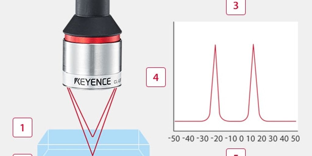
Advanced Metrology Techniques
Advanced metrology techniques involve precise measurements and assessments of the wafer and its components. These techniques help in detecting even the smallest defects, ensuring that only the best chips move forward in the production process. This leads to higher efficiency and reliability in chip manufacturing.
Efficiency and Reliability Improvements
Efficiency and reliability improvements are achieved through continuous monitoring and advanced testing methods. By using these methods, manufacturers can reduce waste, lower costs, and produce higher-quality chips. This not only benefits the manufacturers but also the end-users who receive more reliable and efficient products.
Types of Test Wafers in Semiconductor Testing
In the field of semiconductor testing, various types of test wafers are employed to meet specific manufacturing and quality assurance needs. Each type of test wafer, whether it’s a monitor, dummy, defect, or short loop, plays a distinct role in maintaining high standards in semiconductor testing. These wafers, along with the use of wafer probers and comprehensive chip and die tests, contribute significantly to the production of reliable and high-quality semiconductor products.
Cost-Effective Performance in Wafer-Level Packaging
Innovative inspection techniques for 3D structures and wire bonds are essential for overcoming challenges in wafer-level packaging. These methods ensure that even the smallest defects are detected early, saving both time and resources. Additionally, thermal management strategies for 2.5D integration play a crucial role in maintaining the performance and longevity of semiconductor devices.
Data provenance and predictive analytics are also instrumental in improving final test yields. By tracking the history and origin of data, manufacturers can identify patterns and predict potential issues before they become significant problems. This proactive approach not only enhances the reliability of the devices but also reduces costs associated with rework and failures.
Knowledge transfer across the supply chain is another key factor driving continuous improvement. When best practices and lessons learned are shared among different stakeholders, it leads to more efficient processes and better overall performance. This collaborative effort ensures that the entire industry benefits from advancements in technology and methodologies.
Wafer-Level Burn-In: Ensuring Reliability
Wafer-level burn-in is a crucial step in ensuring the reliability of semiconductor devices. By catching defects early, we help improve yield, reduce testing costs, and enhance overall product reliability. This process involves subjecting wafers to stress conditions that simulate real-world usage, identifying potential failures before they reach the end user.
Challenges in Wafer-Level Packaging
One of the significant challenges in wafer-level packaging is determining the best testing solutions for the next generation of semiconductors. Even when the die has been packaged, there is a complex trade-off between how much to spend on the final test of the package versus the cost to the user or supplier if the device fails while in use. Standardization efforts, particularly in chiplet IP, along with industry collaboration and talent development, are essential.
Integration of Multiple Dies
Integrating multiple dies into a single package presents its own set of challenges. Ensuring that each die functions correctly and reliably when combined is critical. This requires advanced testing techniques and collaboration across the supply chain to ensure that all components work seamlessly together.
Future Innovations in Nanotechnology
The future of wafer-level burn-in lies in the advancements in nanotechnology. As devices become smaller and more complex, new testing methods will be required to ensure reliability. Innovations in this field will continue to drive improvements in semiconductor performance, making devices more efficient and dependable.
Optimizing Manufacturing Processes with Wafer Level Testing
The semiconductor industry is on the brink of a major transformation with the introduction of advanced wafer testing equipment. These innovations are not only improving chip quality but also setting new standards for efficiency and reliability in chip manufacturing. From in-die monitoring to advanced metrology, the sector is experiencing a significant shift.
Advanced Metrology
Advanced metrology techniques are crucial for maintaining high standards of quality and efficiency in semiconductor manufacturing. These methods involve precise measurements and regular monitoring to ensure that every chip meets the required specifications. Statistical Process Control (SPC) is one such strategy that provides a systematic approach to process monitoring, helping to fine-tune process parameters and maintain optimal performance.
Data-Driven Strategies
Data-driven strategies play a vital role in optimizing manufacturing processes. By analyzing data collected during wafer testing, manufacturers can identify trends and patterns that indicate potential issues. This proactive approach allows for timely interventions, reducing the likelihood of defects and improving overall product quality. In today’s manufacturing processes, there are a plethora of automated test and inspection techniques to find defects and add quality.
Continuous Improvement Across Supply Chain
Continuous improvement is essential for staying competitive in the semiconductor industry. By implementing a culture of continuous improvement, manufacturers can regularly assess and enhance their processes. This involves not only addressing current issues but also identifying opportunities for future improvements. Collaborative efforts across the supply chain ensure that every step, from raw material procurement to final product delivery, is optimized for maximum efficiency and quality.
Adapting Wafer Level Testing to Customer-Specific Needs
Customization and adaptability in semiconductor testing are crucial for meeting customer-specific needs and solving new problems. Supported by strong data management systems, these advancements ensure that each customer’s unique requirements are met, boosting overall satisfaction and performance.
Conclusion
In conclusion, the advancements in wafer-level testing are reshaping the semiconductor industry. These new technologies are making chips better and more reliable. From in-die monitoring to smart data analysis, these tools help find and fix problems faster. They also make the manufacturing process smoother and more efficient. As we move forward, these innovations will continue to push the boundaries, making chips even more powerful and dependable. The future of semiconductor manufacturing looks bright, thanks to these cutting-edge testing methods.
Frequently Asked Questions
What is wafer level testing?
Wafer level testing is a process used in semiconductor manufacturing to test individual chips on a wafer before they are cut and packaged. This helps in identifying defects early and ensures better quality and reliability of the final product.
Why is in-die monitoring important?
In-die monitoring is crucial because it allows for real-time observation of the chip’s performance during the manufacturing process. This helps in detecting and correcting issues immediately, leading to improved chip functionality and efficiency.
What are advanced metrology techniques?
Advanced metrology techniques involve using precise measurement tools and methods to evaluate the physical and electrical properties of semiconductor wafers. These techniques help in ensuring that the wafers meet the required specifications and standards.
How does wafer-level packaging improve cost-effectiveness?
Wafer-level packaging improves cost-effectiveness by allowing multiple chips to be packaged together, reducing the need for individual packaging. This not only saves materials and time but also enhances the overall performance and reliability of the chips.
What challenges are faced in wafer-level burn-in?
Wafer-level burn-in faces challenges such as managing thermal stress and ensuring uniformity across all chips. These issues need to be addressed to ensure the reliability and longevity of the chips.
How can wafer level testing be customized for specific needs?
Wafer level testing can be customized by tailoring the testing solutions to meet the specific requirements of different customers. This involves identifying unique improvement opportunities and collaborating on probing solutions to achieve the desired outcomes.