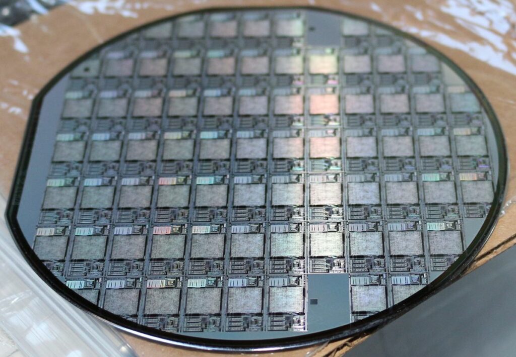
Maximizing Semiconductor Lifespan: The Future of Wafer Level Reliability Testing
As the semiconductor industry marches towards a projected $1 trillion in sales by 2030, wafer level reliability testing becomes increasingly vital. The complexity of fabricating high-performance chips with intricate 3D structures and atomic-scale dimensions necessitates advanced wafer process solutions. These solutions are informed by real-world processing data and accelerated modeling to ensure faster design iterations and enhanced reliability. Addressing technology gaps, talent shortages, supply chain disruptions, and environmental concerns are pivotal in shaping the future of semiconductor longevity.
Key Takeaways
- The semiconductor industry is on the brink of a significant sales milestone, with the need for robust wafer level reliability testing to support this growth.
- Closing technology gaps and overcoming talent shortages are critical for improving wafer level testing and ensuring the reliability of semiconductors.
- Supply chain disruptions and environmental impacts are major considerations in the advancement of wafer level reliability testing.
- Innovations in wafer processing, such as 3D structure fabrication and atomic-scale techniques, are key to enhancing the longevity of semiconductors.
- The economic implications of wafer level testing are profound, affecting sales projections, R&D investments, and strategic industry partnerships.
Challenges and Solutions in Wafer Level Reliability Testing
Addressing the Technology Gap
As semiconductor sales soar towards the $1 trillion mark, the industry faces the critical challenge of closing technology gaps that could hinder progress. Innovative solutions are essential to bridge these gaps and ensure the delivery of high-performance chips with complex 3D structures and atomic-scale dimensions. To address this, companies are focusing on several key areas:
- Knowledge-sharing across companies and with policymakers to create a unified approach to technological challenges.
- Cross-company collaboration to leverage diverse expertise and resources.
- Adaptation strategies such as creating inventory buffers and drafting business continuity plans.
These steps are crucial for maintaining innovation and customer satisfaction, despite the challenges posed by electronics shortages and supply chain issues. The table below summarizes the adaptation strategies for electronics manufacturers:
| Strategy | Description |
|---|---|
| Inventory Buffers | Maintaining safety stocks of scarce materials |
| Business Continuity Plans | Preparing for potential disruptions |
| Reshoring | Identifying areas for bringing production closer to home |
| Local Partnerships | Collaborating with local talent and resources |
| Just-in-Time Workflow | Streamlining work and order flow to reduce waste |
By implementing these strategies, the semiconductor industry can not only overcome the technology gap but also set a resilient model for future growth and innovation.
Tackling Talent Shortages
The semiconductor industry is facing a significant challenge in the form of talent shortages. As the demand for advanced semiconductor technology grows, companies must tackle reasons for current attrition and develop strategies to attract and retain skilled workers. Key to this effort is identifying and accessing untapped talent pools, which can include recent graduates, veterans, and professionals from other industries looking to transition into the semiconductor field.
Enhancing storytelling about the industry and its impact on technology and society can also play a crucial role in attracting talent. By communicating the exciting opportunities and innovations within the semiconductor sector, companies can inspire a new generation of engineers and technicians. Additionally, creating partnerships with educational institutions can ensure a steady pipeline of trained individuals ready to contribute to the industry’s growth.
To summarize, semiconductor companies can fill the expanding talent gap by:
- Drafting business continuity plans that include talent management
- Discovering ways to partner with local talent and educational institutions
- Brainstorming ways to obtain a just-in-time work and order flow
- Enhancing storytelling to showcase the industry’s role in technological advancements
Mitigating Supply Chain Disruptions
In the face of persistent electronics shortages, supply chain diversity and adaptation are critical for companies to maintain their customer base and foster innovation. The Covid-19 pandemic highlighted the fragility of global supply chains, particularly in the semiconductor industry. To address these challenges, several strategies have been proposed:
- Creating inventory buffers or safety stocks of scarce materials
- Drafting business continuity plans
- Diversifying suppliers and supply chain networks
- Leveraging smart technology for forecasting and demand planning
Robust supply chain management is essential, utilizing transparent tools and software to enhance data analytics. This approach enables managers to develop risk management strategies tailored to their specific goals. Diversification of suppliers not only secures materials but also supports smaller providers, promoting equity in the sector and accelerating technological advancement. Smart technologies, such as machine learning, allow for better prediction of demand spikes, optimizing inventory management in an era where warehouse space is at a premium.
Reducing Environmental Impact
The semiconductor industry is increasingly focusing on the environmental impact of its products, from manufacturing to end-of-life disposal. Cradle-to-Gate Life Cycle Assessments (LCAs) are becoming a standard practice to evaluate the environmental footprint of semiconductor chips throughout their production stages. The relative size of the environmental impacts related to Wide Bandgap (WBG) semiconductor chips is expected to grow as other components become smaller and more efficient.
To address these concerns, companies are adopting more thorough and considerate procedures that not only comply with sustainability standards but also provide a competitive edge. This includes optimizing resource use, reducing waste, and implementing recycling programs. The following list outlines key steps for reducing the environmental impact in wafer level reliability testing:
- Establishing sustainability goals and metrics
- Integrating eco-friendly materials and processes
- Enhancing energy efficiency in manufacturing
- Promoting the reuse and recycling of wafers
By taking these steps, corporations can create a stable foundation that ascends an entity above the rest of the competition, ensuring both environmental and economic sustainability.
Advancements in Wafer Processing for Enhanced Reliability
Innovations in 3D Structure Fabrication
The realm of semiconductor fabrication is witnessing a transformative era with the advent of innovations in 3D structure fabrication. These advancements are not only enhancing the precision of microstructures but are also pivotal in reducing the dimensions and cross-sectional areas of components. This is particularly beneficial in applications such as neural recording and stimulation devices, where minimizing tissue damage is crucial.
Recent studies have demonstrated the application of Micro-Electro-Mechanical Systems (MEMS) surface processing techniques to materials that traditionally undergo silicon processing. Techniques such as photolithography, etching, and metallization are refined to achieve micrometer-level precision. The table below summarizes the key techniques and their contributions to the field:
| Technique | Application | Contribution |
|---|---|---|
| Photolithography | Pattern transfer | Enables precise control over microstructures |
| Etching | Material removal | Achieves finer dimensions for intricate designs |
| Metallization | Circuit formation | Enhances electrical connectivity and performance |
These innovations are not only technical milestones but also represent a leap forward in the practical application of semiconductors. The integration of such high-density intracortical recording arrays, for instance, is a testament to the potential of these cutting-edge techniques. As the industry continues to push the boundaries of what’s possible, the future of semiconductor reliability and performance looks brighter than ever.
Atomic-Scale Dimension Techniques
The pursuit of atomic-scale dimension techniques is revolutionizing semiconductor manufacturing, pushing the boundaries of precision and control. Advanced methodologies are now required to handle the intricacies of fabricating devices with features smaller than 2
currently, the industry is witnessing an advance in additive manufacturing of 2D materials, which is pivotal for achieving the desired atomic precision. This process necessitates a dual focus: first, on controlling the synthesis position of 2D materials on the plane, and second, on ensuring adequate connectivity between clusters to facilitate the transport of electric charges.
To illustrate the progress in this domain, consider the following steps involved in atomic-scale manufacturing:
- Deposition
- Etch
- Electron Beam Inspection
- Implant
- Strip
These steps underscore the complexity and the level of detail that goes into creating semiconductors at the atomic scale. As we continue to refine these techniques, the semiconductor industry is poised to meet the ever-increasing demands for smaller, more efficient, and reliable devices.
Real-World Processing Data Integration
The integration of real-world processing data into wafer reliability testing is a pivotal advancement in semiconductor manufacturing. By simulating operational conditions, engineers can anticipate and mitigate potential failures before they occur. This proactive approach is essential for ensuring the longevity and performance of semiconductor devices.
Key stages in semiconductor processing, such as Deposition, Etch, and Implant, are now being closely monitored and optimized using real-time data. The table below illustrates some of the critical processing stages and their respective data integration techniques:
| Processing Stage | Data Integration Technique |
|---|---|
| Deposition | In-situ monitoring |
| Etch | Endpoint detection |
| Implant | Dose control |
Leveraging this data not only accelerates the design process but also enhances the precision of wafer fabrication. As a result, the industry is witnessing a significant reduction in design turns, leading to faster time-to-market for new semiconductor technologies.
Accelerated Modeling for Design Efficiency
The semiconductor industry is rapidly advancing, and with it, the need for accelerated modeling to enhance design efficiency becomes critical. Traditional single-mode reliability models are proving inadequate for accurately predicting mixed-stress aging in advanced devices. This inadequacy highlights the necessity for more sophisticated wafer process solutions that integrate real-world processing data.
To address this, industry leaders are leveraging advanced technologies to enable faster design iterations. For instance, the FlexiCharge AC-DC Power Supply and AEQ series of micro-size HV power converters are examples of modular and configurable technologies that facilitate rapid time to market for medical applications. Such innovations prioritize safety and efficiency, ensuring that the wellbeing of operators and patients remains paramount.
In the context of robust supply chain management, the approach extends beyond medical applications. Industries are exploring the use of alternative materials, like carbon and aluminum, to mitigate sourcing and manufacturing challenges. This strategic shift in material selection is a testament to the industry’s adaptability and its commitment to maintaining a resilient supply chain.
Wafer Level Packaging and Its Role in Semiconductor Longevity
Trends in Wafer Level Component Assembly
The landscape of wafer level component assembly is rapidly evolving, with new technologies enhancing the efficiency and reliability of semiconductor devices. Fan-Out Wafer-Level Packaging (FOWLP) has emerged as a significant trend, offering improved performance and form factor advantages. This technique allows for a higher number of I/O ports without increasing the size of the die, making it a preferred choice for many applications.
Key processes in wafer level component assembly include die attachment, solder balling, and laser-assisted bonding. Each of these processes plays a crucial role in ensuring the structural integrity and electrical performance of the final product. For instance, solder balling is essential for creating robust interconnects in chip scale packaging, while laser-assisted bonding provides precision and strength in material connections.
The market for wafer level packaging services is on an upward trajectory, with a focus on advanced packaging equipment that supports high throughput and automation. The table below highlights the projected market size for FOWLP, indicating its growing importance in the industry.
| Year | Market Size (USD) | CAGR |
|---|---|---|
| 2023 | 2872.25 million | >… |
As the demand for smaller, more powerful electronic devices continues to rise, wafer level component assembly remains a key area for innovation and investment.
The Importance of Wafer Thinning
Wafer thinning is a critical process in semiconductor manufacturing, aimed at reducing the thickness of wafers to enable more compact and efficient packaging. Thinning improves heat management and plays a significant role in the overall performance and longevity of semiconductor devices. By reducing chip stress, thinning also contributes to the reliability of the final product, ensuring that devices can withstand the rigors of everyday use.
The process of wafer thinning involves the removal of backside materials through mechanical polishing and chemical stress relief. This not only aids in creating thinner die for final packaging but also enhances the yield during packaging and dicing operations. As a result, wafer thinning addresses critical industry demands, making it an indispensable step in the production of advanced electronics.
Here are some of the key benefits of wafer thinning:
- Enhanced thermal management
- Reduced mechanical stress on chips
- Improved yield in packaging and dicing
- Facilitation of advanced packaging techniques such as 3D packaging
Advances in Wafer Metal Coating
The field of wafer metal coating is witnessing significant advancements, with the application of various metal stacks via evaporation or sputtering technologies enhancing die performance. These techniques are crucial for the development of semiconductors that are not only more reliable but also capable of meeting the increasing demands of modern technology.
In the realm of advanced packaging equipment, innovations such as electroless plating and electroplating are becoming more prevalent. Electroless plating allows for maskless chemical deposition of metal stacks on wafers, which can serve as intermetallic connections or to enhance product reliability. Electroplating, on the other hand, uses electrodeposition to coat objects with a layer of metal, providing additional benefits such as corrosion resistance and improved electrical conductivity.
The impact of these coating techniques extends beyond the semiconductor industry. For instance, in the medical field, the Revolutionizing Medical Devices with Advanced Coating Techniques report highlights the advantages of advanced coating solutions, including corrosion resistance and promised longevity, which are essential for devices that directly deliver therapeutic treatments.
The Future of 3D Packaging Technologies
The evolution of 3D packaging technologies is pivotal in addressing the increasing demands for higher performance and miniaturization in semiconductors. Navigating the Future of semiconductor packaging requires a deep understanding of both the technological advancements and the materials used, such as the trends in dielectric materials for 3D packaging. These materials are crucial for ensuring reliability and adapting to new packaging architectures.
In the realm of 3D packaging, services like electroless plating, electroplating, and wafer level component assembly are becoming more sophisticated. The integration of advanced equipment, such as laser-assisted bonding and wafer level bumping solutions, is essential for achieving high throughput and fully automated manufacturing. This is not only beneficial for the production scale but also for advanced research and development efforts.
The table below outlines some of the key services and technologies in the 3D packaging sector:
| Service/Technology | Application |
|---|---|
| Electroless Plating | High precision coating |
| Electroplating | Enhanced conductivity |
| Copper Pillar | Structural support |
| Redistribution Layer (RDL) | Circuit rerouting |
| Solder Balling | Electrical connection |
| Laser Assisted Bonding | Precision assembly |
As we look towards the future, the synergy between innovative packaging equipment and specialized services will play a significant role in extending the lifespan of semiconductors. Companies like PacTech are at the forefront, offering tailored solutions that cater to the unique needs of sectors such as aerospace, automotive, and medical devices.
Industry-Specific Wafer Level Testing Applications
Aerospace and Defense Sector Demands
The aerospace and defense sectors face unique challenges in semiconductor reliability, where the stakes are exceptionally high. Ensuring the longevity and robustness of semiconductors is critical, as they are integral to systems where failure can have significant consequences. To address these demands, the industry has developed specific strategies:
- Creating inventory buffers or safety stocks of scarce materials
- Drafting business continuity plans to mitigate disruptions
- Exploring reshoring of critical manufacturing processes
- Partnering with local talent to bolster innovation
- Streamlining just-in-time work and order flows for efficiency
These measures aim to rise above the persistent electronics shortages that have been exacerbated by events such as the Covid-19 pandemic. Supply chain diversity and adaptation are now at the forefront of industry priorities, ensuring that customer bases are maintained and innovation is not stifled by supply constraints. The use of alternative materials, such as carbon and aluminum in remote-operated vehicles, exemplifies the innovative approaches being taken to achieve supply chain resilience.
Automotive Industry Requirements
The automotive industry is facing unprecedented challenges in maintaining the reliability of semiconductor components, which are integral to the modern vehicle’s functionality. Ensuring the longevity of these components is critical, as they are used in safety-critical systems, infotainment, and advanced driver-assistance systems (ADAS).
To meet these stringent requirements, automotive-grade wafers must undergo rigorous testing protocols that simulate extreme operating conditions. This includes thermal cycling, mechanical stress testing, and exposure to corrosive environments. The following table summarizes key automotive testing standards and their purposes:
| Standard | Test Type | Purpose |
|---|---|---|
| AEC-Q100 | Temperature Cycling | Assess thermal endurance |
| AEC-Q101 | Mechanical Stress | Evaluate structural integrity |
| AEC-Q200 | Corrosive Environment | Test for resistance to corrosion |
In addition to adhering to these standards, manufacturers are exploring innovative testing methods to further enhance the reliability of semiconductors in the automotive sector. Collaboration with suppliers and investment in cutting-edge testing equipment are pivotal in driving the industry forward and ensuring that the vehicles of tomorrow are both safe and reliable.
Consumer Electronics and Wearables
The integration of semiconductors into consumer electronics and wearables has revolutionized the way we interact with technology. Reliability testing at the wafer level is crucial to ensure that these devices can withstand the rigors of daily use. Manufacturers are constantly seeking ways to improve the durability and performance of components such as wearable sensors and flexible thin-film transistors.
Recent advancements have led to the development of energy-smart ribbons that not only harvest energy but also store it, making devices more efficient and self-sustaining. The table below highlights key areas of focus for wafer level reliability testing in consumer electronics:
| Focus Area | Description |
|---|---|
| Wearable Sensors | Ensuring functionality under stress and varying conditions. |
| Flexible Electronics | Testing for mechanical endurance and flexibility. |
| Energy Harvesting Components | Verifying efficiency and storage capabilities of new materials. |
| Transparent Thin-Films | Assessing transparency and conductivity for display purposes. |
As the demand for smaller, more powerful devices grows, so does the need for rigorous testing protocols. This ensures that the latest innovations in consumer electronics are not only cutting-edge but also reliable and safe for everyday wear.
Medical Devices and Life Sciences
The integration of wafer level testing in the medical devices and life sciences sectors is pivotal for ensuring the reliability and safety of critical healthcare equipment. Wafer electrical testing attains a superior level of accuracy, which is essential for devices that require high precision, such as analytical instruments and medical lasers.
In the realm of life sciences, the application of semiconductor technology spans a wide range of instruments, from mass spectrometers to electron microscopes (SEM). These devices rely on the flawless operation of semiconductor components, which is why advanced wafer level reliability testing is not just beneficial but necessary.
The table below outlines some of the key medical and life science applications of semiconductor technology:
| Application Area | Device Type | Importance |
|---|---|---|
| Analytical Instruments | Mass Spec, SEM | Precision Analysis |
| Electrosurgery | HIFU, RF | Non-Invasive Procedures |
| Medical Lasers | Surgical, Opthalmic | Targeted Treatments |
| Patient Care | Infusion Pumps, Dialysis | Continuous Monitoring |
As the demand for sophisticated medical devices grows, the semiconductor industry must continue to innovate and improve wafer level testing methods to meet the stringent standards of the medical field.
The Economic Impact of Wafer Level Testing on the Semiconductor Market
Projecting Sales and Market Growth
The semiconductor industry is on the cusp of a significant transformation, with sales projections indicating a robust growth trajectory. As semiconductor sales approach the $1 trillion level by 2030, the market is poised to witness a substantial upswing from the current $600 million benchmark. This growth is contingent upon the industry’s ability to navigate a series of critical challenges, including the closure of technology gaps, the resolution of talent shortages, and the mitigation of supply chain disruptions, all while minimizing the environmental footprint of production processes.
According to a recent Deloitte report, specific end markets such as PCs and smartphones are expected to rebound with a 4% growth in 2024, following a downturn in the previous year. This anticipated resurgence underscores the importance of reliable and advanced wafer level testing to ensure the quality and longevity of semiconductors in these devices.
The economic implications of wafer level testing are far-reaching, influencing not only the semiconductor market but also related sectors. For instance, the medical device industry, particularly in areas like cardiac ablation, is projected to experience a Compound Annual Growth Rate (CAGR) of over 13% from 2023 to 2035. This growth is driven by an aging population and the trend towards minimally invasive procedures, which demand high-performance, miniaturized semiconductor components.
| Year | Projected Sales Growth (%) | Notable Market Trends |
|---|---|---|
| 2024 | 4 | PC and smartphone sales rebound |
| 2030 | Significant | $1 trillion sales level, aging population impact |
| 2035 | Over 13 (medical devices) | Increase in cardiac ablation procedures |
Strategic foresight into these market dynamics is essential for stakeholders to make informed decisions and capitalize on emerging opportunities. The semiconductor industry’s growth is not only a testament to technological innovation but also a reflection of its critical role in powering the future across various sectors.
Cost-Benefit Analysis of Reliability Testing
The intricate balance between ensuring semiconductor reliability and managing costs is a pivotal aspect of the industry. Balancing reliability against cost is becoming more difficult as chip complexity surges and devices become increasingly domain-specific. This necessitates a nuanced cost-benefit analysis that considers not only the direct costs but also the hidden costs and tradeoffs inherent in integrated circuit (IC) quality.
A comprehensive cost-benefit analysis should include the following considerations:
- Initial investment in reliability testing equipment and processes
- Operational costs, including labor and maintenance
- Potential cost savings from reduced warranty claims and customer support
- Long-term benefits of customer satisfaction and brand reputation
The economic implications of wafer level reliability testing are substantial, influencing both the upfront investment and the downstream benefits. By meticulously evaluating these factors, manufacturers can make informed decisions that optimize both quality and profitability.
Investment in Research and Development
Investing in research and development (R&D) is a strategic priority for semiconductor companies aiming to enhance product performance and reduce production costs. This proactive approach not only addresses immediate technical challenges but also fosters long-term innovation and competitiveness in the market.
R&D initiatives are pivotal in overcoming electronics shortages by exploring alternative materials and processes that are less vulnerable to supply chain disruptions. By focusing on the development of eco-friendly and accessible technologies, companies can mitigate the risks associated with scarce resources and fluctuating market demands.
The following list outlines key areas where R&D investments can make a significant impact:
- Creating inventory buffers for critical materials
- Drafting comprehensive business continuity plans
- Identifying opportunities for reshoring production
- Collaborating with local talent and academia
- Implementing just-in-time work and order flows
These efforts are supported by various grants and programs worldwide, demonstrating the global commitment to advancing semiconductor technology through sustained R&D.
Strategic Partnerships and Collaborations
In the semiconductor industry, strategic partnerships and collaborations are pivotal for innovation and market expansion. These alliances often lead to shared technological advancements, pooling of R&D resources, and access to new markets. For instance, partnerships between semiconductor companies and academic institutions can accelerate the development of cutting-edge wafer level testing techniques.
Key collaborations also exist between semiconductor manufacturers and equipment suppliers, ensuring that the testing equipment evolves in tandem with semiconductor technology. This symbiosis is crucial for maintaining the pace of innovation required to meet the demands of various industry sectors.
- Joint ventures and mergers provide financial and technological synergies.
- Cross-licensing agreements allow for the sharing of patents and intellectual property.
- Collaborative research projects can lead to breakthroughs in reliability testing methods.
- Strategic alliances with end-users help tailor testing protocols to specific industry needs.
The table below highlights the benefits of such collaborations:
| Benefit | Description |
|---|---|
| Enhanced Innovation | Shared R&D leads to more robust testing methods. |
| Cost Efficiency | Combined resources reduce overall R&D expenditure. |
| Market Expansion | Partnerships open up new sectors and geographical markets. |
| Risk Mitigation | Shared investment reduces individual company risk. |
Conclusion
As the semiconductor industry approaches a pivotal $1 trillion milestone, the importance of wafer level reliability testing becomes ever more critical. The future of semiconductors hinges on our ability to refine wafer process solutions, leveraging real-world data to enhance modeling and accelerate design iterations. With the advent of sophisticated 3D structures and atomic-scale dimensions, the industry must innovate relentlessly to ensure the longevity and performance of chips. Addressing technology gaps, talent shortages, supply chain stability, and environmental impact will be key to sustaining growth and reliability. Ultimately, the advancements in wafer level testing and burn-in processes will not only drive semiconductor resilience but also shape the future of electronics, impacting sectors from aerospace to medical, and powering the next generation of consumer technology.
Frequently Asked Questions
What are the main challenges in wafer level reliability testing?
The main challenges include addressing the technology gap, tackling talent shortages, mitigating supply chain disruptions, and reducing the environmental impact of semiconductor production.
How are advancements in wafer processing enhancing reliability?
Innovations include 3D structure fabrication, atomic-scale dimension techniques, integration of real-world processing data, and accelerated modeling for design efficiency.
What role does wafer level packaging play in semiconductor longevity?
Wafer level packaging, including component assembly, wafer thinning, and metal coating, is crucial for protecting the semiconductor from physical and environmental damage, thus extending its lifespan.
How does wafer level testing differ across industries?
Different sectors like aerospace, automotive, consumer electronics, and medical devices have specific requirements for reliability and performance, leading to tailored wafer level testing applications.
What is the economic impact of wafer level testing on the semiconductor market?
Wafer level testing contributes to market growth by ensuring the reliability of semiconductors, which is critical for consumer trust and product longevity. It also influences investment in research and development.
What are some recent innovations in wafer level testing?
Recent innovations include the use of micro- and nanomanufacturing techniques for probe fabrication, advances in 3D packaging technologies, and the development of new materials and processes for wafer metal coating.