The Art of Semiconductor Engineering: From Silicon to Systems
The semiconductor industry is a complex and ever-evolving field that spans from the development of materials to the integration of systems. This article, ‘The Art of Semiconductor Engineering: From Silicon to Systems,’ delves into the intricacies of semiconductor engineering, exploring the advancements in materials, design challenges, collaborative efforts within the ecosystem, manufacturing innovations, and the future trends that are shaping the industry. Drawing insights from experts across different domains, the article offers a comprehensive look into the art and science of creating the tiny chips that power our modern world.
Key Takeaways
- The shift to silicon carbide in power semiconductors marks a significant evolution in materials, promising efficiency improvements in power devices.
- The increasing complexity of semiconductor design and integration, such as software-hardware co-design, is addressing the challenges of modern computing demands.
- Collaboration within the semiconductor ecosystem, including the rise of chiplets in automotive, is crucial for innovation and meeting specialized market needs.
- Manufacturing advancements, such as backside power delivery for 2nm devices, are key to sustaining the rapid pace of semiconductor progress.
- Future semiconductor trends predict further integration, such as the potential universality of the UCIe standard, shaping the direction of the industry.
The Evolution of Semiconductor Materials
David Sempek on Power Semis Usher In The Silicon Carbide Era
The era of silicon carbide in power semiconductors marks a significant shift in the materials used in the industry. Silicon carbide (SiC) is now heralded as a superior alternative to traditional silicon in power devices, offering higher efficiency, faster switching speeds, and greater thermal conductivity. This transition is not just a leap in material science but also a response to the growing demands of high-power applications such as electric vehicles and renewable energy systems.
The advantages of SiC over silicon can be encapsulated in a few key points:
- Higher breakdown electric field: SiC’s ability to withstand high voltages is notably superior to that of silicon, making it ideal for high-voltage applications.
- Thermal conductivity: SiC dissipates heat more effectively, which is crucial for power devices that operate at high temperatures.
- Bandgap: The wider bandgap of SiC allows for devices that can operate at higher temperatures and voltages.
The adoption of SiC is not without its challenges, however. The cost of SiC wafers and the complexity of manufacturing SiC-based devices are hurdles that the industry is actively working to overcome. As the technology matures and scales, these barriers are expected to diminish, paving the way for broader adoption and integration into various sectors.
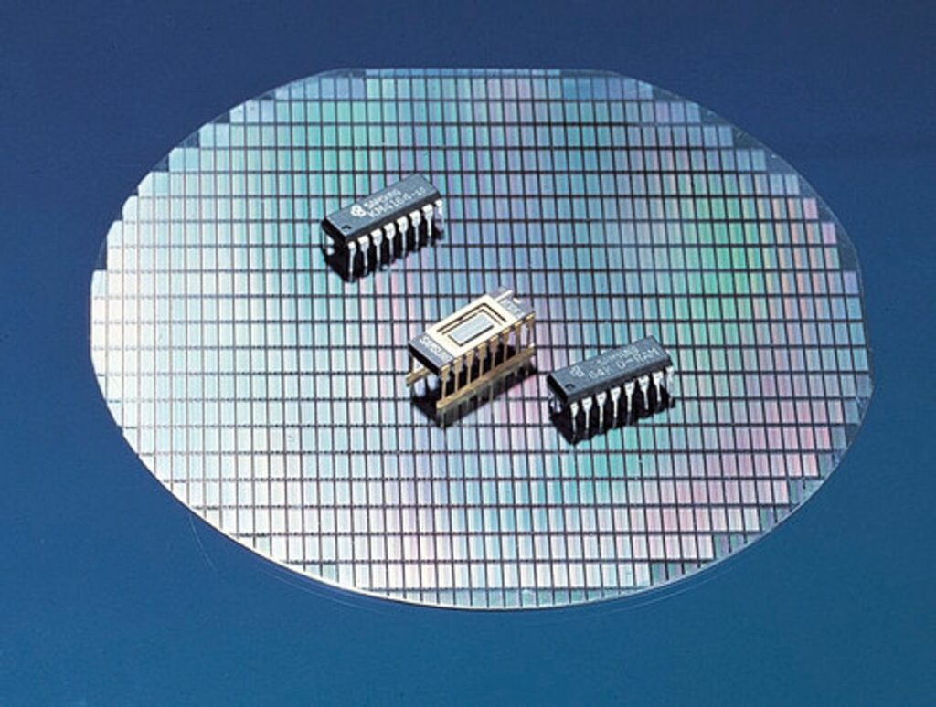
CdrFrancis Leo on Will There Be Enough Silicon Wafers?
The semiconductor industry is facing a pivotal question: Will there be enough silicon wafers to meet the growing demand? CdrFrancis Leo highlights the concerns as the industry scales up to meet the needs of an increasingly digital world. The production of silicon wafers is not just about quantity; it involves maintaining quality at scale, which is a complex challenge given the precision required in semiconductor manufacturing.
The challenges in power semiconductors, as mentioned by David Sempek, resonate here as well. Thermal dissipation, new design rules, and other factors are not only concerns for traditional chips but also for the silicon wafers they are built upon. As the industry evolves, the demand for silicon wafers expands, raising questions about the sustainability of current production methods and the potential need for alternative materials or processes.
To understand the scope of this issue, consider the following points:
- The increasing complexity of chip designs requires higher quality wafers.
- Advancements in technology lead to thinner and larger diameter wafers, pushing the limits of current manufacturing capabilities.
- The shift towards electric vehicles and renewable energy solutions is driving up the demand for power semiconductors, which rely heavily on silicon wafers.
The industry must address these concerns collaboratively to ensure a steady supply of silicon wafers. This will involve investment in new technologies, exploration of alternative materials, and perhaps most importantly, a concerted effort to improve yield and efficiency in wafer production.
Nikolay on Nanoimprint Finally Finds Its Footing
As the semiconductor industry continues to innovate, Nanoimprint lithography (NIL) emerges as a pivotal technology, enabling the cost-effective fabrication of intricate patterns. This method, which can create features ranging from tens of microns down to sub-micron and nano-scales, is particularly advantageous for applications requiring high pattern fidelity and throughput.
The adoption of NIL has been gradual, but recent advancements suggest a firm establishment in the semiconductor manufacturing process. The technology’s ability to produce patterns at a lower cost compared to traditional lithography positions it as a key player in the next generation of semiconductor devices.
Conference insights, such as those from the ‘Novel Patterning Technologies 2024’ at SPIE, highlight the growing relevance of NIL. The table below encapsulates the potential impact of NIL on various semiconductor applications:
| Application Area | Impact of NIL |
|---|---|
| Photonic Devices | Enhanced precision and scalability |
| Bio-sensors | Increased sensitivity and specificity |
| Data Storage | Higher density at reduced costs |
The journey of NIL from a niche technique to a mainstream manufacturing solution underscores the dynamic nature of semiconductor engineering. It is a testament to the industry’s relentless pursuit of innovation and efficiency.
Design and Integration Challenges
Karl Stevens Logic Designer on Software-Hardware Co-Design Becomes Real
The convergence of software and hardware design, often referred to as software-hardware co-design, is no longer a distant concept but a tangible reality in the semiconductor industry. The integration of these two disciplines is crucial for optimizing system performance and efficiency, particularly in the context of complex architectures like those involving Compute Express Link (CXL) memory disaggregation.
In the realm of CXL memory disaggregation, a design tool think tank is essential to navigate the intricacies of software-hardware co-design. This collaborative approach is exemplified by the proposed CXL-ANNS, which aims to enable scalable services for approximate nearest neighbor search (ANNS). Such innovations underscore the need for a holistic view of system design, where software and hardware are developed in tandem to achieve billion-scale efficiencies.
The following points highlight the significance of software-hardware co-design:
- It facilitates the creation of more efficient and powerful computing systems.
- Co-design approaches can lead to innovations like CXL-ANNS, which address specific challenges in data-intensive applications.
- A design tool think tank can provide the necessary foresight and expertise to guide the development of co-designed systems.
Jim Handy on MRAM Getting More Attention At Smallest Nodes
As the semiconductor industry pushes the boundaries of miniaturization, MRAM (Magnetoresistive Random-Access Memory) is gaining traction at the smallest nodes. This emerging technology is being heralded for its potential to combine the speed of SRAM with the non-volatility of flash memory, making it an attractive option for future memory solutions.
The interest in MRAM is not just theoretical; industry leaders are actively exploring its integration into various applications. The table below highlights the key advantages of MRAM over traditional memory types:
| Feature | MRAM Advantage |
|---|---|
| Speed | Comparable to SRAM |
| Non-volatility | Retains data without power |
| Endurance | Higher write cycles |
| Scalability | Suitable for smaller nodes |
With these benefits, MRAM could play a crucial role in the development of more efficient and compact devices. However, the journey from the lab to the fab is fraught with challenges. Material compatibility, manufacturing processes, and cost considerations must all be addressed before MRAM can become a mainstream memory technology.
Lucas on Hybrid Bonding Basics: What Is Hybrid Bonding?
Hybrid bonding represents a significant leap forward in semiconductor packaging technology. The distinguishing feature of hybrid bonding is that it is bumpless, moving away from traditional solder-based bump technologies to establish direct copper-to-copper connections. This method offers numerous advantages, including finer pitch, improved electrical performance, and the potential for greater circuit density.
The process of hybrid bonding can be broken down into several key steps:
- Surface preparation, where wafers are cleaned and made ready for bonding.
- Activation of the surfaces to be bonded, often involving plasma treatment to enhance adhesion.
- Alignment of the wafers, which must be precise to ensure proper bonding.
- Bonding of the wafers at room temperature, followed by annealing to strengthen the bond.
- Inspection and testing to verify the integrity of the bonds.
As the industry continues to push the boundaries of what’s possible in semiconductor design, hybrid bonding is poised to play a pivotal role in the next generation of integrated circuits.
The Semiconductor Ecosystem and Collaboration
Dp on Specialization Vs. Generalization In Processors
The semiconductor industry stands at a crossroads where the decision between specialization and generalization in processor design could shape the future of computing. Specialized processors, tailored for specific tasks, offer optimized performance and efficiency, while general-purpose processors provide broader flexibility.
-
Specialized Processors:
- High efficiency for specific tasks
- Potential for lower power consumption
- Custom design can lead to longer development times
-
General-Purpose Processors:
- Versatile, capable of handling a variety of workloads
- Easier to program for a wide range of applications
- May not achieve the same level of optimization as specialized processors
The debate is not just about performance; it’s also about the economic and practical aspects of processor production. As the industry evolves, the balance between these two paradigms will likely continue to shift, influenced by emerging technologies and market demands.
Jerry Magera on Why Chiplets Are So Critical In Automotive
The automotive industry’s shift towards more advanced and integrated electronic systems has made chiplets an essential component in modern vehicles. Chiplets, which are smaller, modular pieces of an integrated circuit, allow for greater flexibility and scalability in automotive design. This modular approach enables manufacturers to update individual components without redesigning the entire system, crucial for keeping pace with rapid technological advancements.
The key factors to enable automotive chiplet interoperability include standardization, interconnect technologies, communication protocols, power, and thermal management. These elements are vital for ensuring that chiplets from different vendors can work together seamlessly within a vehicle’s electronic ecosystem. The table below outlines the primary considerations for chiplet integration in automotive applications:
| Factor | Importance |
|---|---|
| Standardization | Ensures compatibility and interchangeability |
| Interconnect Technologies | Facilitates communication between chiplets |
| Communication Protocols | Enables data exchange and functionality |
| Power Management | Critical for reliability and efficiency |
| Thermal Management | Maintains performance and prevents overheating |
As the industry continues to evolve, the role of chiplets is expected to expand, with collaboration between semiconductor companies and automotive manufacturers becoming increasingly important. The development of industry-wide standards will be a key driver in the widespread adoption of chiplets in automotive systems.
Valerio Del Vecchio on Security Becoming Core Part Of Chip Design — Finally
The integration of security features into the very fabric of chip design marks a significant shift in the semiconductor industry. Valerio Del Vecchio’s insights underscore the growing recognition that security cannot be an afterthought in a world increasingly dependent on digital technologies. As chips become the backbone of critical systems, from automotive to healthcare, ensuring their integrity is paramount.
Several factors contribute to this paradigm shift:
- The rise of Internet of Things (IoT) devices, which expands the attack surface.
- Increasingly sophisticated cyber threats that target hardware vulnerabilities.
- Regulatory pressures and consumer demand for data protection.
The industry’s response has been to bake security into the chip design process, a move that is as much about protecting end-users as it is about safeguarding the reputation and liability of chip manufacturers. This proactive approach is evident in the collaboration between hardware engineers and cybersecurity experts, aiming to create systems that are resilient by design.
Innovations in Semiconductor Manufacturing
Allen Rasafar on Backside Power Delivery Gears Up For 2nm Devices
The semiconductor industry is on the brink of a significant shift as backside power delivery is poised to be implemented at the 2nm node by the top foundries. This advancement is expected to revolutionize the efficiency and speed of switching in semiconductor devices, marking a pivotal moment in chip design and functionality.
Backside power delivery involves routing power through the backside of the wafer, as opposed to the traditional front-side approach. This method offers several advantages:
- Reduced signal interference, enhancing overall chip performance.
- Improved power distribution, which is crucial for the increasing complexity of modern chips.
- Potential for better heat dissipation, addressing one of the major challenges at smaller nodes.
As the industry gears up for this transition, the implications for future semiconductor designs are profound. The integration of backside power delivery at the 2nm scale will set a new standard for what is possible in power efficiency and chip architecture.
Richard Collins on Too Much Fab And Test Data, Low Utilization
The semiconductor industry is awash with data, yet the utilization of this vast resource is often suboptimal. Richard Collins highlights a critical issue: the overwhelming amount of fab and test data that fails to be fully leveraged. This underutilization represents a missed opportunity for enhancing efficiency and driving innovation.
To address this challenge, several strategies can be implemented:
- Establishing more sophisticated data analytics frameworks.
- Integrating AI/ML algorithms to sift through and make sense of the data.
- Promoting cross-functional collaboration to ensure data is shared and used across different departments.
By adopting these approaches, semiconductor companies can transform data from an underused asset into a powerful tool for competitive advantage.
AKC on Gearing Up For Hybrid Bonding
As the semiconductor industry approaches the 2nm technology node, hybrid bonding is becoming a pivotal technique for device integration. Hybrid bonding offers a path to higher bandwidth and lower power consumption, crucial for next-generation chips. This method allows for the direct bonding of wafers or die without the need for an interposing layer, enabling finer pitch connections and 3D stacking capabilities.
The process of gearing up for hybrid bonding involves several key steps:
- Ensuring surface planarity and cleanliness to facilitate strong bonds.
- Precise alignment of wafers or die to achieve the required connection accuracy.
- Developing robust processes for testing and inspection to maintain high yields.
The transition to hybrid bonding is not without its challenges, including the need for new equipment and the refinement of existing processes. However, the potential benefits in terms of performance and form factor make it a critical area of focus for manufacturers looking to stay at the forefront of semiconductor technology.
Future Trends and Predictions
Kumar Venkatramani on Predicting The Future For Semiconductors
In the ever-evolving landscape of semiconductor technology, Kumar Venkatramani’s insights stand out as a beacon for what’s to come. His predictions are not just educated guesses; they are based on a deep understanding of market trends, technological advancements, and the intricate dance between supply and demand.
Venkatramani emphasizes the importance of innovation in sustaining the industry’s growth. He points to the rise of hybrid bonding and chiplet designs as key areas where we can expect significant developments. These technologies are not only pushing the boundaries of what’s possible in terms of performance but are also crucial for overcoming current manufacturing challenges.
Looking ahead, Venkatramani suggests that the industry should brace for a wave of changes. He highlights the potential of AI-driven MEMS and sensors, which are set to revolutionize various applications, from automotive to healthcare. Moreover, the anticipation of record-breaking fab equipment spending signals a robust future for semiconductor manufacturing, with a forecast reaching $137 billion by 2027.
Jenn Mullen on Shattered Silos: 2024’s Top Technology Trends
In the dynamic landscape of semiconductor technology, Jenn Mullen highlights the breaking down of traditional barriers in her discussion on 2024’s top technology trends. Technological innovation is now increasingly intertwined with global challenges, such as climate change and disaster response. The industry’s focus is shifting towards creating solutions that are not only technologically advanced but also socially responsible and accessible.
The SEMI 3D & Systems Summit recently spotlighted trends that are shaping the future of semiconductors, including hybrid bonding and chiplet design, with a strong emphasis on environmental sustainability. This reflects a broader industry movement towards integrating eco-friendly practices into the core of semiconductor manufacturing processes.
As we look ahead, the SEMI reports predict a surge in fab equipment spending, reaching a record $137 billion by 2027. This investment is indicative of the sector’s commitment to innovation and growth, even as it navigates the complexities of supply chain management and evolving market demands. The semiconductor community continues to thrive on collaboration and knowledge sharing, as evidenced by the wealth of insights shared across various platforms, from SEMI blogs to industry strategy symposiums.
Spike on Is UCIe Really Universal?
The Universal Chiplet Interconnect Express (UCIe) is poised to revolutionize the semiconductor industry by establishing a standardized framework for chiplet integration. This open industry standard aims to foster a vibrant ecosystem where chiplets from various suppliers can seamlessly interconnect, potentially leading to high-performance, power-efficient three-dimensional system-in-package (SiP) solutions. However, the question remains: is UCIe truly universal?
The promise of UCIe lies in its ability to enable a modular approach to design, where different functionalities can be mixed and matched to create tailored solutions for specific applications. This could lead to significant advancements in fields such as artificial intelligence, where specialized processing units are often required. Yet, the adoption of UCIe across the industry is not without its challenges. Compatibility, interoperability, and the willingness of companies to embrace this standard are critical factors that will determine its success.
To understand the current landscape, consider the following points:
- The need for a chiplet ecosystem that supports diverse requirements.
- The role of UCIe in promoting design flexibility and innovation.
- The challenges associated with ensuring universal compatibility and adoption.
As the semiconductor industry continues to evolve, the universal applicability of UCIe will be a topic of ongoing discussion and development. Stakeholders must collaborate to address these challenges, ensuring that UCIe can live up to its potential as a cornerstone of future semiconductor architectures.
Conclusion
The journey from raw silicon to sophisticated systems encapsulates the marvel of semiconductor engineering. This article has traversed the intricate landscape of this field, touching upon the innovations and challenges that define the current state of the art. We’ve seen the universal aspirations of UCIe, the ushering in of the silicon carbide era, and the critical role of chiplets in automotive technology. The shift towards software-hardware co-design and the increasing attention to MRAM at the smallest nodes highlight the industry’s dynamic nature. As we look towards the future, with backside power delivery for 2nm devices and the integration of security into chip design, it’s clear that the semiconductor ecosystem continues to evolve, driven by a relentless pursuit of performance, efficiency, and scalability. The insights from industry experts underscore the importance of collaboration, education, and innovation in overcoming obstacles such as substrate shortages, data utilization, and the talent gap. As we stand on the brink of new breakthroughs, from hybrid bonding to AI-driven EDA, the semiconductor industry remains a testament to human ingenuity and the relentless pursuit of progress.
Frequently Asked Questions
What recent advancements have been made in semiconductor materials?
Recent advancements include the ushering in of the Silicon Carbide era for power semiconductors, improvements in nanoimprint technology, and concerns over the sufficiency of silicon wafer supply.
How are software and hardware co-design impacting semiconductor engineering?
Software-hardware co-design is becoming a reality, allowing for more efficient and optimized systems that leverage the strengths of both domains for better performance and functionality.
What role do chiplets play in the automotive industry?
Chiplets are critical in the automotive industry for enabling modularity, improving performance, and reducing costs by allowing the combination of different functionalities into a single package.
What are the challenges associated with semiconductor manufacturing as we approach 2nm devices?
As we gear up for 2nm devices, challenges include managing backside power delivery, dealing with the overwhelming amount of fab and test data, and the increasing complexity of processes like hybrid bonding.
What are some of the major trends predicted for the future of semiconductors?
Major trends include the integration of various technologies, the rise of universal chip interconnect standards such as UCIe, and the ongoing specialization in processor design.
How is the semiconductor industry addressing security concerns in chip design?
Security is becoming a core part of chip design, with a focus on implementing robust security features from the ground up to protect against a range of vulnerabilities and threats.