The Critical Role of Wafer Probe Testing in Quality Assurance
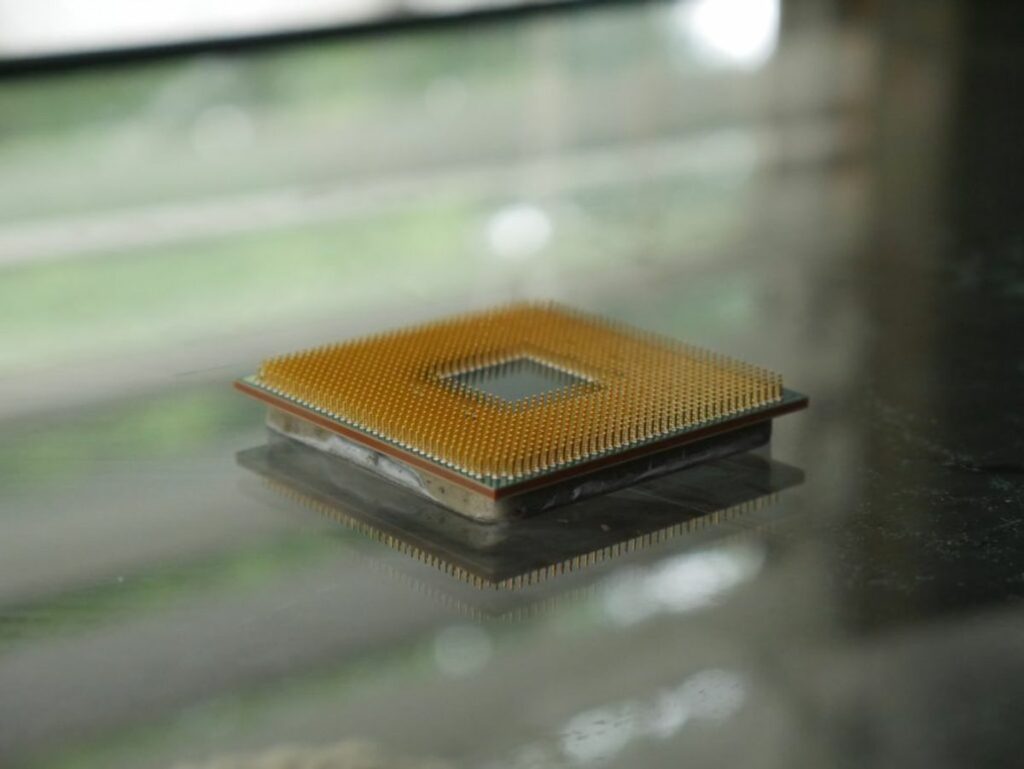
Wafer probe testing plays a pivotal role in the semiconductor manufacturing process, ensuring that each chip meets stringent quality standards before being packaged and shipped. This article explores the critical role of wafer probe testing in quality assurance, highlighting technological advancements, quality assurance strategies, and the impact of emerging technologies on testing protocols. It also delves into the specialized testing requirements of photonic integrated circuits (PICs) and the significance of wafer probe testing for data centers and webscale companies.
Key Takeaways
- EXFO’s OPAL-MD multi-die PIC testing station marks a significant advancement in automated wafer probe testing technology, enhancing accuracy and testing efficiency.
- Quality assurance in semiconductor manufacturing relies heavily on monitoring key parameters and using devices like miniature strip sensors and monitor diodes to detect defects early.
- Wafer probe testing is essential for validating high-speed technologies such as 400G/800G Ethernet, 5G, and fiber networks, ensuring they meet performance standards.
- Automated testing solutions, including EXFO’s role as a PIC ecosystem advisor, are crucial for the high-precision spectral characterization and efficient light coupling in PICs.
- Data centers and webscale companies depend on wafer probe testing to guarantee the infrastructure’s high-speed and reliability, adapting to the demands of virtualized networks and remote PHY.
Advancements in Wafer Probe Testing Technology
Introduction of EXFO’s OPAL-MD Multi-Die PIC Testing Station
The landscape of photonic integrated circuit (PIC) testing is undergoing a significant transformation with the introduction of EXFO’s OPAL-MD. This multi-die PIC testing station is part of the broader OPAL series, which includes solutions for wafer to single-die characterization. The OPAL-MD stands out as the industry’s most accurate and repeatable solution for PIC testing, offering fast and efficient testing capabilities.
EXFO’s commitment to innovation in automated testing is evident in the OPAL-MD’s design. It is a compact and automated probe station that ensures traceable results, setting a new standard for PIC testing. The station’s features include:
- Unsurpassed accuracy and repeatability in test results
- High-speed testing efficiency
- Compact form factor suitable for various testing environments
As a key PIC ecosystem advisor, EXFO continues to lead with unique and patented testing capabilities. The OPAL-MD is a testament to their expertise in delivering automated solutions that meet the evolving needs of the industry.
Automated Probe Stations and Their Impact on PIC Testing
The advent of automated probe stations has revolutionized the testing of Photonic Integrated Circuits (PIC). These stations, such as EXFO’s OPAL series, offer unparalleled accuracy and repeatability in PIC testing. The automation of the testing process not only enhances efficiency but also ensures traceability, which is critical for quality assurance in semiconductor manufacturing.
Automated probe stations facilitate a range of tests, from electrical validation to Ethernet testing, across various technologies including 400G/800G, 5G, and fiber testing. The integration of these stations into the testing workflow allows for rapid and reliable characterization of PICs, which is essential for the fast-paced development of photonic technologies.
The following table highlights the capabilities of automated probe stations in PIC testing:
| Feature | Description |
|---|---|
| Accuracy | Industry-leading precision in measurements |
| Repeatability | Consistent results across multiple tests |
| Traceability | Detailed records for quality assurance |
| Efficiency | Fast testing turnaround times |
| Flexibility | Adaptable to various PIC configurations |
The impact of these automated systems is evident in the speed and reliability with which PICs can now be tested, paving the way for advancements in data centers, webscale companies, and network infrastructure.
Passive Component Test Platforms: The CTP-10
The CTP-10 stands as a testament to the evolution of passive optical component testing, offering unparalleled capabilities for Wavelength Division Multiplexing (WDM) components and photonic integrated circuits (PICs). Its precision and versatility make it an essential tool for ensuring the performance and reliability of passive components in a variety of applications.
Key features of the CTP-10 include:
- High-resolution spectral analysis
- Accurate characterization of WDM filters
- Reliable testing of passive PICs
The platform’s automated testing processes not only enhance efficiency but also contribute to a significant reduction in human error, leading to more consistent and dependable quality assurance outcomes. As the demand for high-performance optical components grows, the CTP-10’s role in maintaining industry standards becomes increasingly vital.
Quality Assurance Strategies in Semiconductor Manufacturing
Monitoring Key Parameters to Prevent Defects
In the realm of semiconductor manufacturing, monitoring key parameters is essential for ensuring the integrity of the final product. Parameters such as voltage, current, and resistance are meticulously measured to identify any defects or inconsistencies that may arise during the production process. Automated test equipment (ATE) is instrumental in this regard, providing the necessary precision and efficiency.
The QA strategy for the ATLAS ITk development exemplifies this approach, focusing on the use of miniature strip sensors and monitor diodes to track deviations in the manufacturing process. These devices offer a compact yet effective means of quality assurance, with the miniature strip sensors mirroring the design of their larger counterparts but at a scale of 1 imes 1 cm^2, and the monitor diodes at 8 imes 8 mm^2.
To further illustrate the importance of these parameters, consider the following table which outlines the skills percentages related to quality assurance in the field:
| Skill | Percentage |
|---|---|
| Data Analysis | 7.63% |
| Test Results | 5.25% |
| RF | 5.02% |
| Test Equipment | 4.84% |
These figures highlight the critical role that various skills play in the QA process, with data analysis leading the charge. It’s clear that a multifaceted approach, combining both hardware and analytical expertise, is key to preventing defects and ensuring the highest standards of quality.
The Role of Miniature Strip Sensors and Monitor Diodes in QA
In the realm of semiconductor manufacturing, quality assurance (QA) is paramount, and the use of miniature strip sensors and monitor diodes plays a critical role. These components are integral in monitoring key parameters to prevent defects and ensure consistency in production.
Miniature strip sensors, or ‘Minis’, measure 1 x 1 cm2 and are primarily utilized for charge collection efficiency (CCE) tests. Monitor diodes, sized at 8 x 8 mm2, are employed for both IV (current-voltage) and CV (capacitance-voltage) tests before and after irradiation. The table below summarizes their applications:
| Component | Size | Test Type | Usage Timing |
|---|---|---|---|
| Monitor Diodes | 8 x 8 mm2 | IV and CV | Pre- and Post-Irradiation |
| Miniature Sensors | 1 x 1 cm2 | CCE | During Production |
The strategic implementation of these devices is supported by various research programs and grants, ensuring that the QA process is both rigorous and effective. By closely monitoring the manufacturing process, deviations are promptly identified and addressed, maintaining the integrity of the semiconductor devices.
Ensuring Quality in Production and Post-Irradiation
In the realm of semiconductor manufacturing, ensuring quality throughout the production process and after irradiation treatments is paramount. The ATLAS ITk Collaboration has developed a comprehensive quality assurance (QA) strategy that includes a detailed irradiation and testing plan. This plan is bolstered by the addition of the China Spallation Neutron Source (CSNS) as a potential QA irradiation site, following a successful feasibility study.
Post-irradiation measurements such as IV (current-voltage), CV (capacitance-voltage), and CCE (charge collection efficiency) are critical. These tests are conducted under controlled cold temperatures after a specific annealing process. The results from these tests at CSNS indicate its suitability as a proton irradiation site for sensor projects, pending formal qualification.
The QA process is underpinned by the use of miniature strip sensors and monitor diodes, which are essential in monitoring key parameters. These devices help in detecting any deviations from the manufacturing process, thereby preventing defects. The table below summarizes the post-irradiation test conditions and the corresponding fluence points studied:
| Test Type | Temperature (C) | Fluence Points (neq/cm^2) |
|---|---|---|
| IV | -8 | 5.1×10^14 to 1.6×10^15 |
| CV | -8 | 5.1×10^14 to 1.6×10^15 |
| CCE | -20 | 5.1×10^14 to 1.6×10^15 |
The Intersection of Wafer Probe Testing and Emerging Technologies
400G/800G Electrical Validation and Ethernet Testing
The evolution of data centers and the increasing demand for high-speed networks have necessitated the development of advanced testing solutions for 400G and 800G Ethernet. Data centers have adopted coherent signaling in full effect for these high-capacity networks, utilizing packages such as OSFP, QSFP-DD, and CFP. The transition from electrical validation to Ethernet testing is a critical step in ensuring the performance and reliability of these networks.
To address these needs, a range of testing solutions have been introduced. These include modular, dual-port 400G testers that allow technicians to test various rates, interfaces, and transceiver types with a single, compact solution. For 800G, solutions like the FTBx-88800 Series provide comprehensive testing capabilities for optical, DCO, and LPO, including support for 800ZR coherent pluggables.
The table below summarizes key testing solutions for 400G and 800G networks:
| Solution | Description |
|---|---|
| FTBx-88480 | Modular, dual-port 400G tester with 112G electrical lanes. |
| FTBx-88800 | 800G test solution with transceiver breakout testing and support for various form factors. |
| BA-4000-L2 | 800G/1.6T traffic and bit analyzer for R&D and manufacturing. |
These solutions not only provide reliable results but also offer the versatility and scalability required to keep pace with the rapid advancements in Ethernet technology.
5G and Fiber Testing: Ensuring Network Readiness
As the world gears up for the widespread deployment of 5G technology, the role of fiber-optic test and measurement devices becomes increasingly critical. These devices are essential for verifying the integrity and performance of the underlying fiber networks that are the backbone of 5G infrastructure. Ensuring network readiness for 5G involves a series of steps, including rigorous testing of both the fiber optics and the wireless components.
The process of fiber testing for 5G readiness typically includes several key stages:
- Validation of the physical infrastructure: This involves checking the fiber cables, connectors, and splices for any physical damage or degradation that could impact performance.
- Performance testing: Measuring key optical parameters such as attenuation, dispersion, and reflectance to ensure that the fiber meets the stringent requirements of high-speed data transmission.
- Network simulation and stress testing: Simulating various network conditions and traffic patterns to evaluate how the fiber network will perform under real-world 5G usage scenarios.
These steps are not only crucial for the initial deployment but also for ongoing maintenance and troubleshooting of the fiber network to support adaptive service assurance solutions. With the right testing protocols in place, network equipment manufacturers (NEMs) and service providers can confidently roll out 5G services, knowing that the fiber infrastructure is robust and reliable.
The Importance of PON and High-Speed Fiber Testing
In the realm of telecommunications, Passive Optical Network (PON) and high-speed fiber testing are pivotal for ensuring the delivery of high-quality network services. PON technology, a cornerstone of fiber-to-the-x (FTTx) systems, requires rigorous testing to guarantee optimal performance and reliability. High-speed fiber testing, on the other hand, is essential for the verification of fiber infrastructure capable of supporting burgeoning data rates.
The following points highlight the significance of PON and high-speed fiber testing:
- Validation of network components: Ensuring that each component meets industry standards and performs as expected.
- Network readiness: Confirming that the network can handle the expected traffic and service levels.
- Troubleshooting and maintenance: Identifying and resolving issues before they impact end-users.
- Future-proofing: Testing for compatibility with upcoming technologies such as 400G/800G Ethernet.
Moreover, the integration of technologies like EVPN and Segment Routing enhances the access network, servicing both multi and single tenant environments. This integration underscores the necessity for comprehensive testing strategies that encompass not only the physical layer but also the network’s feature-rich capabilities.
Automated Testing Solutions for Photonic Integrated Circuits
EXFO’s Role as a PIC Ecosystem Advisor
EXFO stands at the forefront of photonic integrated circuit (PIC) testing, offering unparalleled expertise as a key ecosystem advisor. With unique and patented testing capabilities, EXFO supports the industry from the initial stages of testing bar, die, and wafer-level components to the intricate process of efficiently coupling light onto devices. Their comprehensive approach encompasses the high-precision spectral characterization of both passive and active optical components, ensuring that every aspect of PIC performance meets the highest standards.
As a trusted adviser to network operators and leaders in manufacturing and research, EXFO’s role extends beyond testing solutions. They provide valuable insights into network performance, service reliability, and user experience. Their collaborative efforts are exemplified in the EXFO Exchange platform, which interconnects a customer’s field test ecosystem, optimizing field testing and reporting workflows.
EXFO’s commitment to the PIC sector is further demonstrated through their active participation in industry events and panels, such as the Ethernet Alliance panel session. This engagement with the community highlights their dedication to increasing collaboration, compliance, and field efficiency, ultimately contributing to the advancement of photonic technologies.
High-Precision Spectral Characterization of Optical Components
In the realm of photonic integrated circuits (PICs), high-precision spectral characterization is indispensable for ensuring the performance and reliability of optical components. Optical spectrum analyzers (OSAs) play a pivotal role in this process, providing detailed measurements of optical spectra from which further analysis can be derived.
The use of OSAs in lab and manufacturing settings is widespread, encompassing a variety of applications such as testing WDM components and assessing the spectral properties of PICs. The table below outlines some of the key equipment used in spectral characterization:
| Equipment | Function |
|---|---|
| Optical Spectrum Analyzers | Measure optical spectra |
| Tunable Laser Sources | Provide variable wavelengths |
| Tunable Optical Filters | Adjust spectral selectivity |
| Optical Power Meters | Quantify optical power |
Ensuring the accuracy of these measurements is critical, as they directly impact the quality assurance of the final product. Advanced OSAs offer features like high resolution and wide dynamic range, which are essential for capturing the nuances of optical signals. As technology progresses, the demand for more sophisticated spectral analysis tools will continue to grow, highlighting the importance of continuous innovation in this field.
Efficient Light Coupling onto Devices
The integration of light and electronics through photonic integration is a pivotal advancement in the realm of data transfer. Silicon photonics, a leader in this field, enables faster and more efficient communication. Efficient light coupling onto devices is essential for maximizing the performance of photonic integrated circuits (PICs). This process involves precise alignment and optimization of light sources to the photonic devices, ensuring minimal loss and peak functionality.
EXFO’s automated testing solutions play a crucial role in this aspect, offering a suite of tools for the high-precision spectral characterization of optical components. These tools are designed to facilitate the coupling of light onto PICs with high accuracy, which is critical for the overall performance of the system. The following list highlights key aspects of efficient light coupling:
- Accurate alignment of light sources to PICs
- Minimization of optical losses during coupling
- Optimization of coupling parameters for peak performance
- Use of advanced testing equipment for validation
Researchers have developed new integration techniques that are revolutionizing the industry. These advancements are not only enhancing the efficiency of data transfer but also paving the way for next-generation optics, such as QSFP-DD and OSFP, to be tested and validated with precision.
The Role of Wafer Probe Testing in Data Centers and Webscale Companies
Data Center Infrastructure and Fiber Characterization
In the realm of data centers, the characterization of fiber infrastructure is a cornerstone for ensuring high-speed data transmission and reliable network performance. As data centers evolve to accommodate increasing traffic demands, the role of fiber characterization becomes even more pivotal.
Fiber characterization involves a series of tests to assess the quality and performance of the fiber optic cables. These tests include, but are not limited to, Optical Time-Domain Reflectometer (OTDR) testing, chromatic dispersion, polarization mode dispersion, and spectral attenuation. The results of these tests are crucial for guaranteeing that the fiber links meet the stringent specifications required for modern data transmission standards such as 400G/800G Ethernet.
To illustrate the importance of these tests, consider the following table which outlines key parameters monitored during fiber characterization:
| Test Parameter | Purpose |
|---|---|
| OTDR Testing | Identifies fiber faults and splice losses |
| Chromatic Dispersion | Ensures signal integrity over distance |
| Polarization Mode Dispersion | Mitigates data signal impairments |
| Spectral Attenuation | Measures loss of signal strength |
Furthermore, the simulation of fiber latency and link performance is essential, especially in data centers hosting AI technology. Accurate simulation helps network device manufacturers to anticipate and mitigate issues that could impact the efficiency of data processing and the delivery of services.
The Demand for High-Speed and Reliable Ethernet Solutions
In the era of big data analytics, Internet of Things (IoT), and an ever-increasing online presence, data centers are at the heart of the digital economy. The need for 400G/800G Ethernet solutions is critical to support the surge in data traffic and to ensure seamless connectivity across networks, including submarine links.
The following table highlights the key areas where high-speed Ethernet solutions are essential:
| Area | Importance of High-Speed Ethernet |
|---|---|
| Data Centers | Backbone for cloud services and storage |
| Fiber Characterization | Ensuring integrity and performance of fiber networks |
| Fiber Monitoring | Real-time surveillance to prevent outages |
| Submarine Networks | Vital for global internet connectivity |
EXFO’s advanced testing solutions are designed to meet these demands, providing comprehensive Ethernet/IP testing capabilities. From lab and manufacturing to field deployment, ensuring high-quality communications with low latency is paramount. As networks evolve with technologies like SDN/NFV and wireless innovations, the role of wafer probe testing in maintaining the quality of Ethernet solutions becomes even more significant.
Adapting to Virtualized Networks and Remote PHY
The evolution of data centers and webscale companies towards virtualized networks and Remote PHY architectures is a testament to the ongoing transformation in the telecommunications industry. These advancements necessitate robust wafer probe testing to ensure the integrity and performance of photonic integrated circuits (PICs) that underpin these technologies.
With the integration of Remote PHY, data centers are moving towards a more distributed architecture. This shift allows for greater scalability and flexibility, but also introduces new challenges in maintaining signal integrity and system reliability. Wafer probe testing plays a pivotal role in addressing these challenges by providing early detection of potential issues at the wafer level.
To illustrate the critical parameters monitored during wafer probe testing in this context, consider the following table:
| Parameter | Importance | Testing Method |
|---|---|---|
| Signal Integrity | Ensures data transmission accuracy | Electrical-to-optical validation |
| System Reliability | Prevents system failures | End-to-end Ethernet testing |
| Scalability | Facilitates network growth | High-speed testing (400G/800G) |
As networks continue to evolve, the demand for high-speed and reliable Ethernet solutions only grows. Wafer probe testing is indispensable in meeting these demands, ensuring that as networks become more virtualized and complex, their foundational components remain robust and dependable.
Conclusion
In summary, wafer probe testing stands as an indispensable pillar in the realm of quality assurance for semiconductor devices. The meticulous process of monitoring, developing, and releasing test programs, coupled with the deployment of cutting-edge automated probe stations like EXFO’s OPAL series, underscores the commitment to precision and efficiency. The integration of technologies such as 400G/800G Ethernet, 5G, and fiber testing into wafer probe testing workflows not only enhances the reliability of photonic integrated circuits (PICs) but also propels the industry towards a future of high-speed, high-quality network infrastructure. As we have seen, the rigorous QA strategies employed in projects like the ATLAS ITk development and the innovative solutions provided by EXFO for automated PIC testing, reflect the critical role that wafer probe testing plays in ensuring that the devices at the heart of our digital world meet the highest standards of performance and durability.
Frequently Asked Questions
What is wafer probe testing and why is it critical for quality assurance?
Wafer probe testing is a process where electrical tests are conducted on a silicon wafer to identify defects and ensure that the integrated circuits (ICs) meet the required specifications. This step is critical for quality assurance because it allows manufacturers to verify the functionality and reliability of ICs before they are packaged, which helps to prevent costly recalls and ensures customer satisfaction.
How have advancements in wafer probe testing technology impacted semiconductor manufacturing?
Advancements such as EXFO’s OPAL-MD Multi-Die PIC Testing Station and automated probe stations have significantly improved the accuracy, repeatability, and efficiency of wafer probe testing. These technologies have enabled faster testing times, better defect detection, and overall improved quality control in semiconductor manufacturing.
What role do miniature strip sensors and monitor diodes play in quality assurance?
Miniature strip sensors and monitor diodes are used to monitor key parameters during the manufacturing process to prevent defects. They provide valuable data that helps in identifying deviations and ensuring that the production process remains within the specified quality standards.
Why is photonic integrated circuit (PIC) testing important for emerging technologies?
PIC testing is crucial for emerging technologies such as 5G, high-speed fiber optics, and Ethernet solutions because PICs are integral components in these systems. Ensuring that PICs are tested accurately and efficiently is vital for the performance and reliability of these advanced technologies.
How are data centers and webscale companies affected by wafer probe testing?
Data centers and webscale companies rely heavily on high-speed and reliable Ethernet solutions, as well as robust fiber infrastructure. Wafer probe testing ensures the quality of the components that make up these systems, which is essential for maintaining the performance and uptime required by these companies.
What is the significance of automated testing solutions in quality assurance?
Automated testing solutions streamline the testing process, reduce human error, and increase the throughput of quality assurance testing. This is particularly important for high-volume production environments where maintaining consistency and efficiency is key to meeting the demands of the market while ensuring high quality.