The Future of Wafer Probing
In the dynamic world of semiconductor manufacturing, wafer probing stands as a critical process for assessing the electrical performance of each die on a wafer. This article explores the current landscape and future of wafer probing, delving into technological advancements, market dynamics, and innovative solutions that are shaping this essential field.
Key Takeaways
- Wafer probing is integral to semiconductor manufacturing, enabling precise electrical testing of individual dies.
- Technological advancements such as automation, digitization, and miniaturization are enhancing the efficiency and capability of wafer probing systems.
- Emerging technologies and innovative probe card designs are poised to address current challenges and improve testing accuracy.
- Market trends indicate a growing demand for more sophisticated wafer probing solutions to accommodate smaller and more complex devices.
- Strategic recommendations for stakeholders involve embracing these advancements to stay competitive and meet the evolving demands of the semiconductor industry.
Overview of Wafer Probing
Definition and Significance
Wafer probing is a critical process in semiconductor development and manufacturing, where each die on a wafer is electrically tested to ensure quality and functionality. This process is essential for identifying defects before further processing, making it a cornerstone in the production of reliable integrated circuits.
Core Components of Wafer Probing Systems
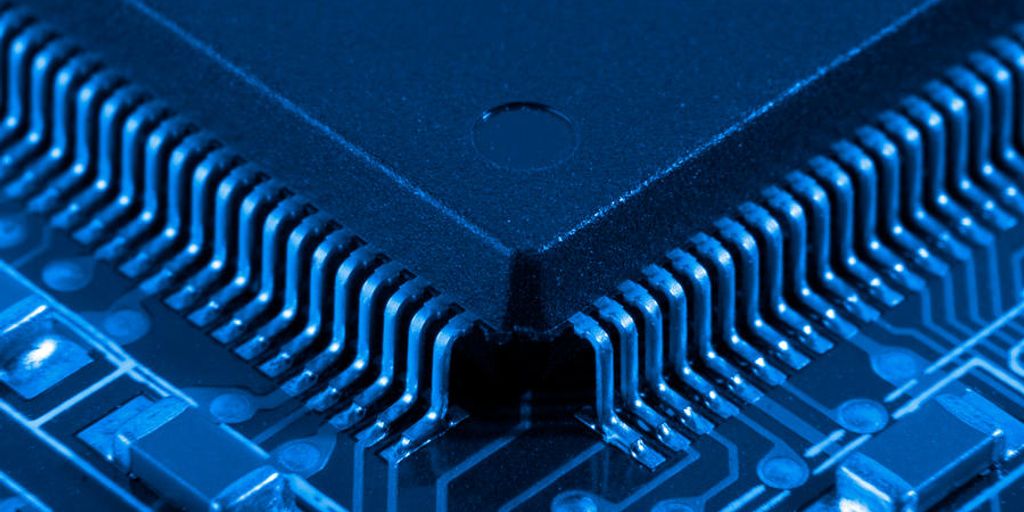
The core components of wafer probing systems include the probe card, the prober, and the tester. The probe card is equipped with metallic elements or needles that make contact with the wafer’s surface, establishing an electrical path essential for testing. The prober holds the wafer securely during testing, while the tester processes the electrical data transmitted through the probe card.
Current Challenges in Wafer Probing
Current challenges in wafer probing include the need for higher accuracy and the reduction of testing time. Innovations like automated wafer probing systems have significantly reduced the time required for fault analysis, enhancing efficiency in semiconductor manufacturing.
Technological Advancements in Wafer Probing
Automation and Digitization
Automation and digitization in wafer probing have revolutionized the testing process, enhancing both accuracy and efficiency. Automated systems ensure precise placement of probes and rapid testing across wafers, reducing human error and increasing throughput.
Miniaturization and Integration
The trend towards miniaturization and integration has led to the development of more compact and integrated probe systems. These advancements allow for more efficient use of space and resources, and improve the overall functionality of wafer probing systems.
Emerging Technologies in Wafer Probing
Emerging technologies, such as AI and machine learning, are being incorporated into wafer probing to further enhance testing capabilities. These technologies enable predictive maintenance, improved decision-making, and greater adaptability to complex testing scenarios.
Wafer Probing in Semiconductor Manufacturing
Role in Quality Assurance
Wafer probing is crucial for ensuring the quality and reliability of semiconductor devices. It involves testing each die on a wafer to identify defects early in the manufacturing process. This step is vital for maintaining the high standards required in modern technology.
Impact on Production Efficiency
Wafer probing not only enhances product quality but also significantly boosts production efficiency. By detecting faulty dies before further processing, it reduces waste and increases the yield of usable chips.
Future Trends in Semiconductor Testing
The future of semiconductor testing through wafer probing is expected to see innovations in automation and miniaturization. These advancements will further refine the precision and speed of testing, making it an even more integral part of semiconductor manufacturing.
Innovations in Probe Card Design
Material Advancements
In the realm of probe card design, material advancements have significantly enhanced performance and durability. Innovations such as the use of advanced ceramics and composite materials have led to improvements in heat resistance and electrical insulation, crucial for maintaining accuracy in high-temperature testing environments.
Electrical and Mechanical Improvements
Electrical and mechanical enhancements in probe cards have focused on increasing the precision and reliability of contact points. Features like controlled overdrive and reduced temperature drifts ensure consistent performance across various testing conditions. Additionally, the integration of smart repair concepts and diagnostic functions has improved the longevity and serviceability of probe cards.
Customization for Specific Needs
Customization for specific testing requirements is a key trend in probe card design. This includes the development of probe cards with variable geometries and functionalities tailored to different semiconductor device types. For instance, vertical style technology is employed for efficient probing in multi-row pad layouts, addressing the limitations of traditional cantilever probes.
Market Dynamics of Wafer Probing
Current Market Trends
The wafer probing market is witnessing significant shifts, primarily driven by the increasing demand for efficient and precise testing solutions. Trends such as automation, digitization, and miniaturization are shaping the landscape, enhancing the capabilities of wafer probing systems to handle smaller die sizes and more complex semiconductor devices.
Growth Drivers
Key factors propelling the growth of the wafer probing market include cross-industry collaborations and technological innovations. Partnerships with semiconductor manufacturers, wafer fab equipment suppliers, and testing solution providers are crucial. These collaborations help in developing cutting-edge prober technology, offering comprehensive solutions that drive market expansion.
Challenges and Barriers
Despite the growth, the market faces challenges such as the high cost of advanced probing technologies and the need for continuous innovation. Companies must navigate these barriers to maintain competitiveness and meet the evolving demands of the semiconductor industry.
Case Studies: Wafer Probing Success Stories
Industry Leaders in Wafer Probing
Keysight Technologies has been at the forefront of wafer probing advancements, particularly in the integration of automation and precision measurement technologies. Their success stories often highlight the efficiency and accuracy improvements in semiconductor testing, making them a benchmark in the industry.
Breakthroughs in Testing Methods
Recent breakthroughs have significantly enhanced the capabilities of wafer probing systems. For instance, the development of non-contact probing methods has reduced the risk of damaging delicate wafer surfaces, thereby improving the reliability of the tests.
Adoption of New Technologies
The semiconductor industry has seen a rapid adoption of new technologies in wafer probing, driven by the need for higher throughput and better yield rates. Innovations such as AI-driven predictive maintenance and real-time data analysis are now common, reflecting a shift towards more intelligent and efficient manufacturing processes.
Future Outlook for Wafer Probing
Predictions for Technological Developments
The wafer probing industry is poised for significant technological advancements, with a focus on automation and digitization. These improvements are expected to enhance the precision and speed of semiconductor testing, catering to the demands of next-generation chips.
Potential Market Expansions
The market for wafer probing is anticipated to expand, driven by the increasing complexity of semiconductor devices and the need for more sophisticated testing solutions. The projected CAGR from 2021 to 2028 is 6.40%, indicating robust growth in the sector.
Strategic Recommendations for Stakeholders
Stakeholders should consider the following strategies to capitalize on the opportunities presented by the evolving market:
- Leverage cross-industry collaborations to develop innovative probing technologies.
- Focus on the integration of IoT, 5G, and AI technologies to meet future testing requirements.
- Explore ecosystem partnerships and disruptive product launches to stay competitive.
Conclusion
As we look to the future of wafer probing, it is evident that the field is poised for significant advancements in efficiency, accuracy, and integration capabilities. The trends towards miniaturization, automation, and digitization are set to redefine the landscape of semiconductor testing. These developments will not only enhance the precision of testing but also expedite the overall manufacturing process, ensuring that the semiconductor industry can meet the growing demands for more complex and smaller devices. The continuous innovation in wafer probing technology is crucial for maintaining the pace of advancements in the broader field of microelectronics and will play a pivotal role in the evolution of next-generation electronic devices.
Frequently Asked Questions
What is wafer probing?
Wafer probing is a process in semiconductor manufacturing where each die on a wafer is electrically tested using a set of very thin pins that contact designated probe pads on the die. This process is crucial for assessing the electrical performance of integrated circuits before further processing.
Why is wafer probing important in semiconductor manufacturing?
Wafer probing is vital for ensuring the quality and reliability of semiconductor devices. It allows manufacturers to identify defects and evaluate the electrical properties of components at an early stage, which helps in maintaining high standards in the production of microelectronics.
How has automation impacted wafer probing?
Automation in wafer probing has led to increased efficiency, accuracy, and speed of testing. Automated systems can precisely place and control the testing process, which is essential for mass production testing of semiconductor devices.
What are the benefits of miniaturization in wafer probing?
Miniaturization in wafer probing supports the testing of smaller die sizes and higher levels of integration. This is crucial as the demand for smaller, more complex semiconductor devices grows, requiring more precise and integrated testing solutions.
What is a probe card and how does it function?
A probe card is a device used in wafer probing that connects to a tester to establish an electrical path between the wafer and the tester. It uses metallic elements or needles to contact the pads of integrated circuit chips on the wafer, transmitting electrical data and test parameters necessary for assessment.
What future trends are expected in wafer probing technology?
Future trends in wafer probing technology include further advancements in automation, digitization, and integration. There is also a focus on developing more sophisticated probe cards and testing methods to keep up with the evolving complexity of semiconductor devices.