Understanding Silicon Wafer Semiconductor Technology and Its Applications
Silicon wafers are the unsung heroes of modern technology. These thin slices of silicon are essential for making the electronic devices we use every day. From smartphones to computers, silicon wafers are at the heart of it all. This article will explore what silicon wafers are, how they are made, their different types and sizes, and their many applications. We’ll also look at the future trends and challenges in silicon wafer technology.
Key Takeaways
- Silicon wafers are crucial for making electronic devices like smartphones and computers.
- There are different types of silicon wafers, including monocrystalline and polycrystalline.
- The manufacturing process of silicon wafers involves several steps, such as doping and photolithography.
- Silicon wafers are used in various applications, including microchips, transistors, and MEMS devices.
- Future trends in silicon wafer technology focus on miniaturization, new materials, and sustainability.
The Basics of Silicon Wafer Semiconductor Technology
Silicon wafers are a fundamental component in the technology industry, serving as the substrate material for microelectronic devices. These thin slices of semiconductor material form the basis for integrated circuits (ICs), which are used in a wide range of electronic devices, from smartphones and computers to advanced medical equipment and aerospace technology.
What is a Silicon Wafer?
Imagine a perfectly flat and thin disc, often just a fraction of a millimeter thick, made from highly purified silicon. These are silicon wafers, and they serve as the canvas upon which the intricate designs of modern semiconductor devices are etched.
How Silicon Wafers are Made
The process of making silicon wafers starts with raw silicon, which is derived from sand. This silicon is then purified and melted down. The molten silicon is formed into a large, cylindrical shape called an ingot. Once the ingot is cooled, it is sliced into thin wafers. These wafers are then polished to achieve a smooth surface, ready for use in semiconductor manufacturing.
Key Properties of Silicon Wafers
Silicon wafers are known for their unique electrical properties, high thermal conductivity, and low coefficient of thermal expansion. These properties make them ideal for crafting essential electronic components like transistors and diodes. Their high purity is crucial for ensuring the performance and reliability of the devices they are used in.
Types and Sizes of Silicon Wafers
Monocrystalline vs. Polycrystalline Silicon Wafers
Silicon wafers can be either monocrystalline or polycrystalline. Monocrystalline wafers are made from a single, continuous crystal structure, which makes them highly efficient for electronic applications. On the other hand, polycrystalline wafers consist of multiple small silicon crystals, making them less efficient but cheaper to produce.
Standard Sizes and Thicknesses
Silicon wafers come in various standard sizes, typically measured in inches or millimeters. Common sizes include:
- 2 Inch (50.8 mm)
- 3 Inch (76.2 mm)
- 4 Inch (100 mm)
- 5 Inch (125 mm)
- 6 Inch (150 mm)
- 12 Inch (300 mm)
The thickness of these wafers can also vary, but they are generally thin to allow for better heat dissipation and electrical performance.
Specialty Silicon Wafers
Specialty silicon wafers are designed for specific applications and can have unique properties. These include:
- P-Type Silicon: Doped with elements like boron to create positive charge carriers.
- N-Type Silicon: Doped with elements like phosphorus to create negative charge carriers.
- Undoped Silicon: Pure silicon with no added elements.
- Float Zone Silicon: High-purity silicon created using the float zone process.
- Single Side Polished: Polished on one side for specific applications.
- Double Side Polished: Polished on both sides for high-precision applications.
- As-Cut Silicon: Wafers that are cut but not polished.
- Lapped Silicon: Wafers that have been ground to a specific thickness but not polished.
Manufacturing Processes Involving Silicon Wafers
Doping and Oxidation
Doping and oxidation are crucial steps in the manufacturing of silicon wafers. Doping involves adding impurities to the silicon to change its electrical properties. This process is essential for creating p-type or n-type semiconductors. Oxidation, on the other hand, involves growing a layer of silicon dioxide on the wafer’s surface. This layer acts as an insulator and protects the wafer during subsequent processing steps.
Photolithography and Etching
Photolithography and etching are used to create intricate patterns on the silicon wafer. Photolithography involves coating the wafer with a light-sensitive material called photoresist. A mask with the desired pattern is then placed over the wafer, and ultraviolet light is shone through the mask. The exposed areas of the photoresist are then developed, leaving behind a pattern. Etching removes the exposed silicon, creating the desired features on the wafer.
Metallization and Testing
Metallization is the process of depositing metal layers on the silicon wafer to create electrical connections. This is typically done using techniques like sputtering or chemical vapor deposition. Once the metal layers are in place, the wafer undergoes rigorous testing to ensure it meets the required specifications. Testing involves checking for electrical properties, defects, and overall functionality. Any wafers that do not meet the standards are discarded or reworked.
Applications in the Semiconductor Industry
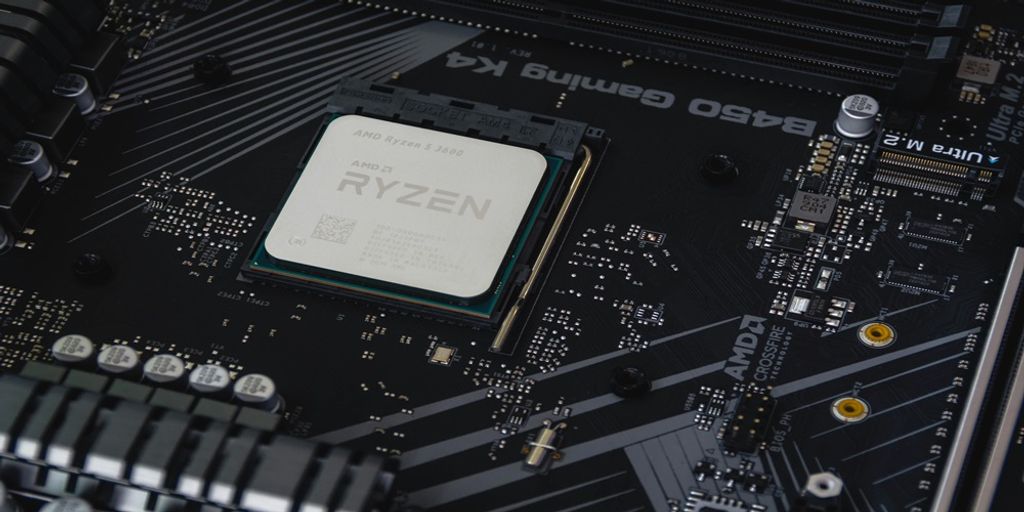
Silicon wafers are the building blocks of semiconductors. They are essential in creating microchips, transistors, and integrated circuits. These components are the heart of modern electronics, making our devices smarter and faster.
Microchips and Integrated Circuits
Microchips and integrated circuits are found in almost every electronic device. From smartphones to computers, these tiny components power our world. Silicon wafers are crucial in their production, providing the foundation for these advanced technologies.
Transistors and Diodes
Transistors and diodes are key elements in electronic circuits. They control the flow of electricity and are used in everything from radios to complex computer systems. Silicon wafers help in making these components more efficient and reliable.
MEMS Devices
Micro-Electro-Mechanical Systems (MEMS) devices are tiny machines that combine electrical and mechanical components. They are used in a variety of applications, including sensors and actuators. Silicon wafers are vital in the manufacturing of MEMS devices, enabling the creation of smaller and more precise components.
Future Trends in Silicon Wafer Semiconductor Technology
As we look ahead, emerging trends and innovations promise to redefine the role of silicon wafers in the semiconductor industry, shaping the future of technology.
Challenges in Silicon Wafer Production
Material Purity and Defects
One of the biggest challenges in making silicon wafers is keeping the silicon pure. Even tiny bits of dirt can mess up the whole process. Maintaining the purity of the silicon is super important because any little defect can cause big problems in the final product. This means that the factories have to be really clean and use special tools to keep everything just right.
Cost and Efficiency
Making silicon wafers costs a lot of money. The process uses a lot of energy and special machines, which makes it expensive. For example, the Siemens process and the Czochralski process both need a lot of energy and special tools. Because of this, companies are always looking for ways to make things cheaper and faster without losing quality.
Environmental Impact
Silicon wafer production uses a lot of resources, including water. Semiconductor manufacturing requires huge amounts of water to form ultrapure water, impacting the local environment and needing innovation and scrutiny. This can hurt the environment if not managed well. Factories need to find ways to use less water and energy to be more eco-friendly. They also need to think about how to recycle materials and reduce waste to help protect the planet.
Conclusion
Silicon wafer semiconductor technology is at the heart of our modern electronic world. These tiny slices of silicon are essential for making everything from microchips to solar cells. They have unique properties that make them perfect for these tasks, like being able to conduct electricity just right and handling heat well. Over the years, the technology has evolved, and now we can make even smaller and more efficient devices. As we move forward, silicon wafers will continue to be a key part of new and exciting technological advancements. Understanding this technology helps us appreciate the incredible devices we use every day.
Frequently Asked Questions
What is a silicon wafer?
A silicon wafer is a thin slice of silicon that serves as the base for building electronic circuits and components. It’s used in making microchips, transistors, and other semiconductor devices.
How are silicon wafers made?
Silicon wafers are made through a process that involves growing a large crystal of silicon, slicing it into thin discs, and then polishing these discs to create a smooth surface.
What are the key properties of silicon wafers?
Key properties of silicon wafers include their ability to conduct electricity, their high purity, and their thermal stability. These properties make them ideal for use in electronic devices.
What are the different types of silicon wafers?
There are mainly two types of silicon wafers: monocrystalline and polycrystalline. Monocrystalline wafers are made from a single crystal, while polycrystalline wafers are made from multiple crystals.
What are the common applications of silicon wafers?
Silicon wafers are commonly used in the semiconductor industry to make microchips, integrated circuits, transistors, and diodes. They are also used in MEMS devices and solar cells.
What are the future trends in silicon wafer technology?
Future trends in silicon wafer technology include advancements in miniaturization, the use of new materials and composites, and efforts towards sustainability and recycling.