Understanding the Benefits of Silicon Carbide Wafer in Electronics
Silicon carbide wafers have emerged as a revolutionary material in the field of electronics, offering a range of unique properties and advantages over traditional silicon wafers. Known for their high thermal conductivity, exceptional hardness, and wide bandgap, silicon carbide wafers are transforming various applications, particularly in power electronics. This article delves into the benefits, applications, and future trends of silicon carbide wafers, providing a comprehensive understanding of their impact on the electronics industry.
Key Takeaways
- Silicon carbide wafers offer high thermal conductivity, exceptional hardness, and a wide bandgap, making them ideal for high-performance applications.
- These wafers are extensively used in power electronics, including electric vehicles, renewable energy systems, and power supplies.
- Compared to silicon, silicon carbide wafers provide higher efficiency, greater durability, and lower energy loss.
- The manufacturing process of silicon carbide wafers involves complex steps such as raw material sourcing, crystal growth techniques, and wafer fabrication.
- Despite their advantages, challenges such as material defects, cost implications, and scalability issues persist in silicon carbide wafer production.
The Unique Properties of Silicon Carbide Wafer
High Thermal Conductivity
Silicon carbide wafers exhibit high thermal conductivity, which makes them ideal for high-power applications. This property allows for efficient heat dissipation, reducing the risk of overheating and improving the overall reliability of electronic devices.
Exceptional Hardness
The exceptional hardness of silicon carbide wafers makes them highly resistant to wear and tear. This durability ensures a longer lifespan for components made from this material, which is particularly beneficial in demanding environments.
Wide Bandgap
Silicon carbide wafers have a wide bandgap, which allows them to operate at higher voltages and temperatures compared to traditional silicon wafers. This characteristic is crucial for applications that require high efficiency and performance under extreme conditions.
Applications of Silicon Carbide Wafer in Power Electronics
Silicon carbide wafers are revolutionizing the field of power electronics, offering significant advantages in various applications.
Electric Vehicles
In the realm of electric vehicle power electronics, silicon carbide wafers are becoming increasingly popular. They provide higher efficiency and better thermal management, which are crucial for the performance and longevity of electric vehicles.
Renewable Energy Systems
Silicon carbide wafers are also making a substantial impact on renewable energy systems. Their ability to handle high voltages and temperatures makes them ideal for use in solar inverters and wind turbine converters, enhancing the overall efficiency and reliability of these systems.
Power Supplies
In power supplies, silicon carbide wafers offer improved efficiency and reduced energy loss. This leads to more compact and lighter power supply units, which are essential for modern electronic devices and industrial applications.
Advantages of Silicon Carbide Wafer Over Silicon
Silicon carbide (SiC) wafers offer significantly higher efficiency compared to traditional silicon wafers. This is primarily due to their ability to operate at higher voltages and temperatures, which reduces energy loss and improves overall system performance. SiC has excellent flexural and tensile strengths and can withstand greater stresses without deformation or rupture.
The exceptional hardness of silicon carbide makes it far more durable than silicon. This durability translates to longer-lasting components that require less frequent replacement, thereby reducing maintenance costs. Additionally, SiC has good chemical stability at room temperature, making it resistant to various environmental factors.
One of the most compelling advantages of silicon carbide wafers is their ability to minimize energy loss. This is achieved through their wide bandgap, which allows for more efficient electrical conduction. As a result, systems utilizing SiC wafers can achieve higher performance levels while consuming less power.
Manufacturing Process of Silicon Carbide Wafer
The manufacturing process of silicon carbide wafers is intricate and requires precision at every stage. Each step requires careful execution to avoid introducing new defects or compromising the wafer’s quality.
Raw Material Sourcing
The process begins with sourcing high-purity raw materials. Silicon carbide is typically derived from a mixture of silicon and carbon, which are then subjected to high temperatures to form the compound. Ensuring the purity of these materials is crucial for the quality of the final product.
Crystal Growth Techniques
Crystal growth is a critical phase in the production of silicon carbide wafers. Techniques such as physical vapor transport (PVT) and chemical vapor deposition (CVD) are commonly used. These methods allow for the formation of large, high-quality silicon carbide crystals, which are essential for the subsequent wafer fabrication steps.
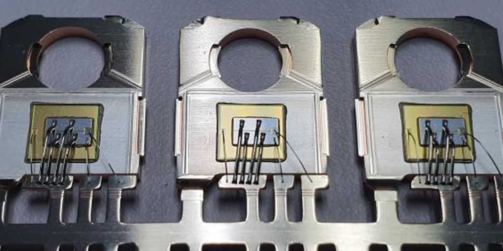
Wafer Fabrication
Post-growth processing involves wafer slicing, grinding, polishing, and surface preparation. Each step requires careful execution to avoid introducing new defects or compromising the wafer’s quality. The wafers are then subjected to various tests to ensure they meet the required specifications before being used in electronic applications.
Challenges in Silicon Carbide Wafer Production
Material Defects
Silicon carbide wafers are prone to various material defects that can significantly impact their performance. These defects include micropipes, dislocations, and stacking faults. Addressing these defects is crucial for improving the quality and reliability of the wafers.
Cost Implications
The production of silicon carbide wafers is an expensive process. High costs are associated with raw materials, advanced manufacturing techniques, and quality control measures. These costs can be a barrier to widespread adoption and scalability.
Scalability Issues
Scaling up the production of silicon carbide wafers presents several challenges. The transition to larger wafer sizes, such as 8-inch wafers, is particularly difficult. Additionally, there is a limited number of 8” wafer suppliers as of 2024, which further complicates the scalability of production.
Future Trends in Silicon Carbide Wafer Technology
Innovations in Material Science
The field of material science is witnessing rapid advancements, particularly in the development of silicon carbide wafers. Researchers are exploring new methods to enhance the quality and performance of these wafers, which could lead to more efficient and durable electronic devices.
Market Growth Projections
According to TrendForce, the SiC power device market is expected to reach USD 5.33 billion by 2026, with its mainstream applications still highly reliant on power electronics. This significant market growth is driven by the increasing demand for high-efficiency and high-performance electronic components.
Potential New Applications
The versatility of silicon carbide wafers opens up numerous potential new applications. These include advanced communication systems, high-frequency radar, and even quantum computing. As the technology matures, we can expect to see innovative uses that leverage the unique properties of silicon carbide.
Environmental Impact of Silicon Carbide Wafer
The production of Silicon Carbide (SiC) wafers is energy-intensive, primarily due to the high temperatures required for crystal growth techniques. However, the efficiency gains in electronic devices using SiC can offset this initial energy expenditure over the product’s lifecycle.
Effective waste management practices are crucial in the SiC wafer manufacturing process. The industry is increasingly focusing on recycling and reusing materials to minimize waste. This not only helps in reducing the environmental footprint but also in lowering production costs.
The advancement of Silicon Carbide semiconductors not only holds promise for enhanced efficiency and performance in electronics but also aligns with global sustainability goals. Companies are investing in green technologies and sustainable practices to ensure that the benefits of SiC wafers are realized without compromising the environment.
Conclusion
In conclusion, the adoption of silicon carbide wafers in the electronics industry marks a significant advancement in technology. These wafers offer superior performance, efficiency, and durability compared to traditional silicon wafers. As the demand for high-power and high-frequency devices continues to grow, silicon carbide wafers are poised to play a crucial role in meeting these needs. Their ability to operate at higher temperatures and voltages makes them ideal for a wide range of applications, from electric vehicles to renewable energy systems. Embracing silicon carbide technology not only enhances device performance but also contributes to the development of more sustainable and energy-efficient electronic systems.
Frequently Asked Questions
What is a silicon carbide wafer?
A silicon carbide wafer is a thin slice of silicon carbide crystal used in the fabrication of electronic components, particularly in high-power and high-frequency devices.
Why is silicon carbide preferred over silicon in power electronics?
Silicon carbide offers higher efficiency, greater durability, and lower energy loss compared to silicon, making it ideal for power electronics applications.
What are the main applications of silicon carbide wafers?
Silicon carbide wafers are primarily used in electric vehicles, renewable energy systems, and power supplies due to their superior performance characteristics.
What challenges are associated with the production of silicon carbide wafers?
The production of silicon carbide wafers faces challenges such as material defects, high costs, and scalability issues.
How is a silicon carbide wafer manufactured?
The manufacturing process involves raw material sourcing, crystal growth techniques, and wafer fabrication, each requiring precise control and advanced technology.
What is the environmental impact of silicon carbide wafer production?
The environmental impact includes energy consumption, waste management issues, and the necessity for sustainability initiatives to mitigate adverse effects.