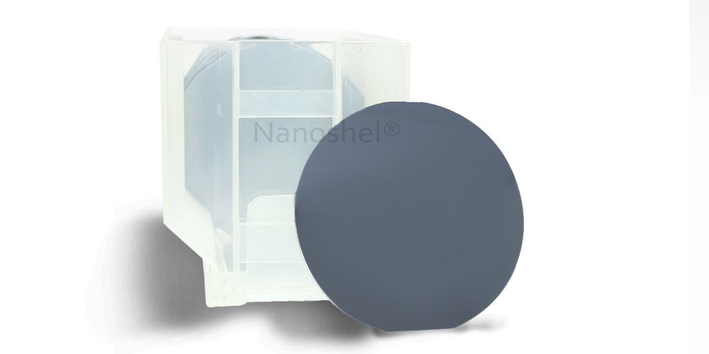
Understanding the Importance of Silicon Carbide Wafer in Modern Electronics
Silicon carbide wafers are becoming a key material in modern electronics. These wafers are known for their unique properties that make them ideal for high-performance applications. From electric vehicles to renewable energy systems, silicon carbide wafers are driving advancements in various fields. This article explores their role, properties, manufacturing processes, and future prospects.
Key Takeaways
- Silicon carbide wafers improve the efficiency of power electronics, especially in electric vehicles and renewable energy systems.
- They have superior thermal conductivity and high breakdown voltage, making them suitable for high-temperature applications.
- The manufacturing process of silicon carbide wafers involves crystal growth, thinning, polishing, and strict quality control.
- Compared to traditional silicon wafers, silicon carbide wafers offer better performance but are more expensive.
- Despite production challenges, silicon carbide wafers have a promising future with potential market growth and innovations in material science.
The Role of Silicon Carbide Wafer in Power Electronics
Silicon carbide (SiC) wafers are becoming essential in power electronics, surpassing traditional silicon semiconductors in areas where efficiency and performance are crucial. SiC devices can handle higher voltages, frequencies, and temperatures, making them ideal for various electronic applications, from industrial motor drives to grid infrastructure.
Thermal and Electrical Properties of Silicon Carbide Wafer
Silicon carbide wafers are known for their superior thermal conductivity. This property allows them to conduct heat much better than traditional silicon wafers, making them ideal for high-power applications. The low thermal expansion coefficient of silicon carbide also means that it doesn’t expand or contract much with temperature changes, ensuring stability in various conditions.
Silicon carbide wafers also boast a high breakdown voltage. This means they can handle higher voltages without breaking down, which is crucial for power electronics. Additionally, they exhibit low power loss, making them more efficient in energy conversion processes. These properties make silicon carbide a desirable material for modern electronics, especially in applications requiring high efficiency and reliability.
Manufacturing Processes of Silicon Carbide Wafers
Crystal Growth Techniques
The first step in making silicon carbide wafers is growing a single crystal. This is done by heating the material to a very high temperature and then cooling it slowly. This process is crucial for creating high-quality wafers.
Wafer Thinning and Polishing
After the crystal is grown, it is sliced into thin wafers using a diamond saw. The wafers are then polished to remove any surface flaws. This makes the wafers smooth and ready for use in electronics.
Quality Control Measures
Quality control is very important in wafer production. Each wafer is checked for defects to make sure it meets the required standards. This step ensures that only the best wafers are used in making electronic devices.
Comparing Silicon Carbide Wafers to Traditional Silicon Wafers
Performance Differences
Silicon carbide (SiC) wafers and traditional silicon wafers have distinct performance characteristics. SiC wafers offer higher efficiency and can operate at higher temperatures compared to silicon wafers. This makes them ideal for high-power applications. On the other hand, silicon wafers are more commonly used due to their lower cost and established manufacturing processes.
Cost Implications
The cost of SiC wafers is generally higher than that of traditional silicon wafers. This is due to the more complex manufacturing processes and the higher cost of raw materials. However, the improved performance and efficiency of SiC wafers can lead to cost savings in the long run, especially in high-power and high-temperature applications.
Suitability for High-Temperature Applications
SiC wafers are particularly well-suited for high-temperature applications. They can withstand temperatures that would cause traditional silicon wafers to fail. This makes them ideal for use in environments where high thermal stability is required, such as in power electronics and aerospace applications.
Applications of Silicon Carbide Wafers in Modern Electronics
Use in High-Frequency Devices
Silicon carbide wafers are essential in high-frequency devices. They can handle high power levels and operate at high temperatures, making them ideal for radio-frequency (RF) applications. Their ability to perform under extreme conditions sets them apart from traditional silicon wafers.
Role in Aerospace and Defense
In aerospace and defense, silicon carbide wafers are used for their durability and efficiency. They are crucial in systems that require reliable performance in harsh environments, such as satellites and military equipment. Their high thermal conductivity and electrical properties ensure stable operation.
Integration in Consumer Electronics
Silicon carbide wafers are also making their way into consumer electronics. They are used in devices that need efficient power management and high performance, such as smartphones and laptops. Their superior properties help in reducing power loss and improving battery life.
Challenges and Future Prospects of Silicon Carbide Wafers
Production Challenges
Producing silicon carbide wafers is not easy. One big problem is keeping the material pure during the whole process. Another issue is the high cost of making these wafers. Finding ways to make the process cheaper and more efficient is very important. Some solutions include improving the production steps, recycling materials, and trying out new materials.
Market Growth Potential
The market for silicon carbide wafers is growing fast. More and more industries are using these wafers because they work better in high-power and high-temperature settings. This means there is a big chance for growth in the future. Companies are investing a lot of money in research to make these wafers even better.
Innovations in Material Science
New ideas in material science are helping to solve some of the problems with silicon carbide wafers. Scientists are always looking for new ways to make these wafers work better and cost less. Some of these new ideas include better ways to grow the crystals and new methods for making the wafers thinner and smoother.
Environmental Impact of Silicon Carbide Wafer Production
Energy Consumption in Manufacturing
The production of silicon carbide wafers is energy-intensive. The processes involved, such as crystal growth and wafer slicing, require a lot of power. Reducing energy consumption is crucial to make the production more sustainable. Manufacturers are exploring ways to use renewable energy sources and improve energy efficiency in their operations.
Waste Management and Recycling
During the wafer slicing and polishing processes, a significant amount of silicon carbide is lost as waste. This waste can be collected and recycled back into the manufacturing process, reducing the need for new raw materials. Recycling not only helps in cutting down costs but also minimizes the environmental footprint of the production process.
Sustainability Initiatives
To address environmental concerns, many companies are adopting sustainability initiatives. These include using eco-friendly materials, reducing emissions, and implementing green manufacturing practices. By focusing on sustainability, the industry aims to lessen its impact on the environment while meeting the growing demand for silicon carbide wafers.
Conclusion
Silicon carbide wafers are truly game-changers in the world of electronics. They offer unique benefits that traditional silicon wafers can’t match, like better thermal conductivity and the ability to handle higher voltages. These features make them perfect for a variety of applications, from powering electric cars to running high-speed trains. As technology keeps advancing, the role of silicon carbide wafers will only grow more important. They are not just a part of modern electronics; they are paving the way for the future.
Frequently Asked Questions
What is silicon carbide wafer?
A silicon carbide wafer is a thin slice of silicon carbide material used in electronics. It has special properties that make it good for high-power and high-temperature applications.
How does silicon carbide improve power electronics?
Silicon carbide wafers help make power electronics more efficient. They reduce power loss and can handle higher voltages and temperatures compared to traditional silicon wafers.
Why is silicon carbide used in electric vehicles?
Silicon carbide is used in electric vehicles because it helps improve the efficiency of the power electronics, which leads to longer battery life and better performance.
What are the thermal properties of silicon carbide wafers?
Silicon carbide wafers have excellent thermal conductivity, meaning they can effectively dissipate heat. This makes them ideal for high-power applications where heat management is crucial.
Are silicon carbide wafers more expensive than silicon wafers?
Yes, silicon carbide wafers are generally more expensive than traditional silicon wafers. However, their superior performance can justify the higher cost in many applications.
What are the challenges in producing silicon carbide wafers?
Producing silicon carbide wafers is challenging due to the complex manufacturing processes involved, such as crystal growth and wafer thinning. Quality control is also crucial to ensure the wafers meet the required standards.