Understanding the Importance of Wafer Probe Testing in Semiconductor Manufacturing
Wafer probe testing is a key part of making semiconductors. It checks each tiny chip on a big wafer to make sure they work right before they get cut and packaged. This step helps find bad chips early, saving time and money.
Key Takeaways
- Wafer probe testing checks each chip on a wafer to make sure they work properly.
- This process helps find and remove bad chips early, saving time and resources.
- Wafer probe testing has evolved from manual methods to advanced automated systems.
- It plays a crucial role in ensuring the quality and reliability of semiconductor devices.
- Technological advancements continue to improve the accuracy and efficiency of wafer probe testing.
Understanding Wafer Probe Testing
Definition and Importance
Wafer probe testing is a key step in making semiconductors. It checks how well each chip on a wafer works before they are cut and packaged. By using probe cards to connect the test system to the wafer, defective chips can be found and removed early, ensuring only the best ones move forward.
Historical Development
Wafer probe testing has come a long way. It started with manual testing of prototype integrated circuits. Over time, it has evolved into an automated process that offers very accurate measurements. This helps in evaluating test element groups (TEGs) made up of transistors, connectors, and other parts.
Key Components Involved
The main parts of a wafer probe testing system include:
- Wafer Chuck: Holds the wafer in place.
- Probe Card: A set of tiny needles that make contact with the wafer.
- Test System: Sends and receives electrical signals to and from the wafer.
These components work together to ensure that each chip is tested for quality before moving on to the next stage of production.
The Role of Wafer Probe Testing in Semiconductor Manufacturing
Ensuring Chip Functionality
Wafer probe testing is essential in making sure that each chip on a wafer works correctly. By testing the electrical performance of individual chips before they are cut and packaged, manufacturers can catch and remove defective chips early. This step is crucial to ensure that only the best-performing chips move forward in the production process.
Resource and Cost Efficiency
Wafer probe testing helps save both resources and money. By identifying faulty chips early, manufacturers can avoid the costs associated with packaging and further processing defective units. This not only reduces waste but also improves overall production efficiency.
Impact on Production Yield
The testing process has a significant impact on production yield. By catching defects early, wafer probe testing increases the number of functional chips produced from each wafer. This leads to higher yields and better use of materials, which is vital for meeting the high demand for semiconductor devices.
Technological Advancements in Wafer Probe Testing
Automation and Precision
The world of wafer probe testing has seen significant changes with the introduction of modern techniques. One major advancement is the use of automated systems that enhance precision and speed. These systems reduce human error and increase throughput, making the testing process more efficient.
Temperature Variability Testing
Temperature variability testing has become a crucial part of wafer probe testing. By simulating different temperature conditions, manufacturers can ensure that chips will perform reliably under various environmental conditions. This type of testing helps in identifying potential issues that could arise due to temperature fluctuations.
Future Trends
The semiconductor industry is rapidly evolving, and new technologies are constantly being developed to improve wafer probe testing. One of the most exciting trends is the integration with Industry 4.0 principles. This includes real-time monitoring, data analytics, and predictive maintenance, which are becoming standard features in modern probe card holders. These advancements are ushering in a new era of intelligent semiconductor testing.
Failure Analysis Through Wafer Probe Testing
Wafer probing is an important part of the analysis of semiconductors in manufacturing. With detailed testing, this process helps to find the main causes of errors in semiconductor devices. The detailed results of the failure analysis help to increase the production process, avoiding the same error in the future and making sure the manufacturing of high-quality and error-free components.
Design Verification and Wafer Probe Testing
Prototype Assessment
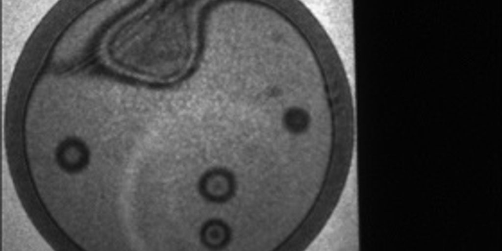
Wafer probe testing is crucial in the early stages of semiconductor development. It helps in evaluating prototype integrated circuits to ensure they meet design specifications. This process involves using an automated wafer probing system to test each die on a wafer. The system places thin pins on designated probe pads, also known as contact pads, to check the electrical properties of the circuits.
Test Element Group (TEG) Evaluation
Another important aspect of wafer probe testing is the evaluation of the Test Element Group (TEG). This group consists of various components like transistors and connectors. Wafer probing offers extremely accurate measurements, which are essential for assessing the reliability of these components under different conditions, including low and high temperatures.
Enhancing Design Reliability
Wafer probe testing plays a significant role in enhancing the reliability of semiconductor designs. By identifying and removing dies that are unsuitable for packaging, manufacturers can ensure that only high-quality components move forward in the production process. This step is vital for maintaining the overall quality and performance of the final product.
Challenges and Solutions in Wafer Probe Testing
Wafer probe testing is essential in the semiconductor industry, but it comes with its own set of challenges. Testing VCSEL devices on wafers presents multiple challenges. One significant requirement is the ability to perform accurate and reliable tests despite various obstacles.
Conclusion
In semiconductor manufacturing, wafer probe testing is like a gatekeeper for quality. By checking each tiny chip on a wafer, engineers can spot problems early and fix them before the chips are used in our devices. This not only saves time and money but also makes sure that the gadgets we use every day are reliable and long-lasting. As technology keeps getting better, the methods and tools for wafer probe testing will also improve, helping the industry keep up with new challenges and demands.
Frequently Asked Questions
What is wafer probe testing?
Wafer probe testing is a process used to check the quality and functionality of semiconductor wafers before they are cut into individual chips. It helps identify any defects early in the manufacturing process.
Why is wafer probe testing important?
Wafer probe testing is important because it ensures that only functional and reliable semiconductor chips move forward in the production process. This helps save time and resources by identifying defects early.
What are the key components involved in wafer probe testing?
The key components involved in wafer probe testing include the probe card, the test system, and the wafer itself. These components work together to test the electrical performance of individual chips.
How has wafer probe testing evolved over time?
Wafer probe testing has evolved from manual probing methods to highly automated systems that offer greater precision and efficiency. Technological advancements have made it possible to test wafers at different temperatures and conditions.
What role does wafer probe testing play in semiconductor manufacturing?
Wafer probe testing plays a crucial role in semiconductor manufacturing by ensuring chip functionality, improving production yield, and enhancing resource and cost efficiency. It helps catch defects early, reducing waste and increasing overall quality.
What are some common challenges in wafer probe testing?
Some common challenges in wafer probe testing include dealing with tiny and delicate components, maintaining precision at high speeds, and testing under various environmental conditions. Innovative solutions and advancements in technology are continuously addressing these challenges.