Understanding the Production and Use of Silicon Wafers
Silicon wafers are integral to the technology industry, serving as the primary base for creating integrated circuits, semiconductor devices, and solar cells. Known for their unique electrical and thermal properties, these wafers must maintain high levels of purity to function effectively. Despite production challenges, innovative manufacturing techniques and global demand continue to drive the evolution and application of silicon wafers.
Key Takeaways
- Silicon wafers are crucial for the production of integrated circuits and semiconductor devices, impacting various sectors.
- High purity levels and specific electrical properties are essential for the optimal performance of silicon wafers.
- Production techniques like the Czochralski process and wafer slicing are fundamental to maintaining wafer quality.
- Innovations in manufacturing aim to reduce costs and enhance sustainability, addressing both economic and environmental concerns.
- Silicon wafers are expanding beyond traditional electronics, finding roles in solar energy, biomedical fields, and other emerging technologies.
The Essential Role of Silicon Wafers in Technology
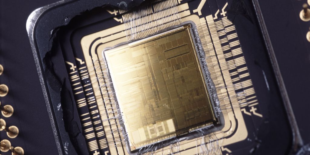
Silicon wafers are pivotal in the technology sector, underpinning the development and functionality of integrated circuits, semiconductor devices, and solar cells. These thin slices of semiconductor material are crucial for semiconductor devices, facilitating the flow of electrical current and enabling essential functions like amplification and switching. Their role extends to the foundation of solar cell production, where their unique properties, such as high thermal conductivity and low thermal expansion, make them ideal for converting solar energy into electrical energy.
Foundation for Integrated Circuits
Silicon wafers form the substrate for microelectronic devices, which are integral to a wide array of electronic devices, from smartphones to advanced medical equipment.
Crucial for Semiconductor Devices
These devices govern the flow of electrical current in electronic circuits, playing a critical role in the functionality of a vast range of technologies.
Key in Solar Cell Production
Their high purity and specific electrical properties are essential in crafting solar cells that efficiently convert solar energy into electrical power, highlighting their importance in sustainable energy solutions.
Properties of Silicon Wafers
High Purity Requirements
High purity is critical for the performance of silicon wafers in semiconductor devices. Any impurities can significantly affect the electrical properties and the overall functionality of the devices. Manufacturers strive to achieve and maintain the highest possible purity levels during production.
Electrical and Thermal Characteristics
Silicon wafers exhibit unique electrical and thermal properties that are essential for their function in technology. Their ability to conduct electricity can be finely tuned through doping, which involves adding impurities to change the electrical characteristics. Additionally, their high thermal conductivity is crucial during the manufacturing process, preventing damage from high temperatures.
Impact of Impurities on Performance
The presence of impurities in silicon wafers can drastically impact their performance. Even trace amounts of contaminants can alter electrical conductivity and thermal properties, leading to failures in semiconductor devices. Ensuring minimal impurity levels is a constant challenge in wafer production.
Production Processes of Silicon Wafers
Czochralski Process
The Czochralski process is a critical method used to grow single crystal silicon. The process begins with melting high-purity polysilicon in a quartz crucible. A seed crystal of silicon is then dipped into the molten mass and slowly withdrawn, promoting the growth of a cylindrical crystal, or boule, of silicon.
Wafer Slicing and Polishing
After the boule is formed, it is sliced into thin discs called wafers using a diamond saw, which is chosen for its hardness and precision. The wafers are then polished to achieve the necessary smoothness and thickness for semiconductor fabrication.
Challenges in Maintaining Purity
Maintaining the purity of silicon wafers throughout the manufacturing process is paramount. Contamination can occur at any stage, from the handling of raw materials to the final polishing of the wafers. Rigorous quality control and clean room environments are essential to minimize impurities and ensure the performance of the final semiconductor devices.
Innovations in Silicon Wafer Manufacturing
Technological Advancements
The relentless pursuit of technological advancements in silicon wafer manufacturing has led to significant improvements in precision and efficiency. Innovations such as enhanced lasers, advanced chemical processes, and increased automation have revolutionized the production landscape. These developments not only improve the quality of wafers but also reduce the occurrence of defects, ensuring higher performance in end-use applications.
Cost Reduction Strategies
To combat the inherently high costs of production, manufacturers have implemented various cost reduction strategies. These include optimizing existing processes, recycling silicon materials, and exploring the use of alternative, less expensive materials. Such strategies are crucial for maintaining competitiveness in the global market and making the technology accessible to a broader range of industries.
Sustainability in Production
Sustainability has become a key focus in the manufacturing of silicon wafers. Efforts to minimize environmental impact include reducing energy consumption during production and implementing waste management practices. The industry is also exploring more sustainable materials and methods that could potentially replace traditional practices, thereby reducing the ecological footprint of silicon wafer production.
Global Demand and Supply Dynamics
Annual Production Figures
The global silicon wafer market is projected to reach nearly $17 billion by 2027, reflecting robust growth driven by technological advancements and expanding applications. Annual production has been steadily increasing, with major transitions in wafer sizes from 200mm to 300mm to accommodate higher efficiency and output.
Growth in Semiconductor Industry
The semiconductor industry’s growth is closely tied to the evolution of silicon wafer technology. As devices become more sophisticated, the demand for larger and more pure wafers grows. This demand fuels investments into new fabrication plants capable of producing these advanced wafers, ensuring a steady supply to meet the industry’s needs.
Supply Chain Considerations
Navigating the supply chain for silicon wafers involves managing the high costs of manufacturing facilities, which can range from $10-20 billion for leading-edge fabs. The limited number of end customers who can afford these costs creates a competitive environment where only a few providers dominate. Careful management of these economic factors is crucial for maintaining a stable supply chain in the face of increasing demand.
Applications of Silicon Wafers Beyond Electronics
Use in Solar Energy
Silicon wafers play a pivotal role in the solar energy sector, primarily in the production of photovoltaic cells. These cells convert sunlight into electricity, and the high purity and efficiency of silicon wafers make them ideal for this application. The global shift towards renewable energy sources has significantly increased the demand for high-quality silicon wafers in solar technologies.
Biomedical Applications
In the biomedical field, silicon wafers are utilized for various diagnostic and therapeutic devices. Their biocompatibility and precise engineering allow for the creation of intricate components used in medical implants and sensors. This integration of silicon technology in medicine is enhancing patient care and treatment outcomes.
Emerging Technological Uses
Silicon wafers are finding new applications in innovative fields such as autonomous vehicles and smart sensors. These applications leverage the unique electrical and thermal properties of silicon wafers to enhance performance and reliability in cutting-edge technologies. The versatility of silicon wafers continues to drive their adoption in various sectors, pushing the boundaries of what is technologically possible.
Future Trends in Silicon Wafer Technology
Research and Development
The relentless pursuit of higher efficiency and lower costs in silicon wafer production is expected to continue. Innovations are likely to focus on enhancing production technologies and materials to meet the growing demands of the tech industry. Key areas include the development of larger wafer sizes and the integration of advanced automation and quality control systems.
Potential New Materials
Exploration of alternative materials that can complement or replace silicon in certain applications is on the rise. These materials are being researched for their potential to offer better performance or unique properties that could revolutionize the industry.
Predictions for Industry Growth
The silicon wafer market is poised for significant growth, with projections suggesting a market size nearing $17 billion by 2027. This growth is driven by the expansion of silicon-based technologies and the scaling up of wafer sizes from 200mm to 300mm, which allows for more circuits per wafer and reduced costs per chip.
Conclusion
Silicon wafers are indispensable in the realm of technology, serving as the backbone for the production of integrated circuits, semiconductor devices, and solar cells. Their unique electrical and thermal properties, coupled with high purity, make them essential for a wide range of applications. Despite the challenges in production, such as maintaining purity and managing costs, innovative solutions have been developed to ensure their efficient and cost-effective production. As the demand for more powerful electronic devices continues to grow, the role of silicon wafers remains crucial, underpinning the ongoing advancements in the technology industry.
Frequently Asked Questions
What are silicon wafers?
Silicon wafers are thin slices of silicon that serve as the substrate for the fabrication of electronic devices. They are produced from ultra-pure silicon through a series of complex processes, including the Czochralski process, wafer slicing, and polishing.
Why are silicon wafers used in the technology industry?
Silicon wafers are fundamental in manufacturing integrated circuits and microchips that power a vast array of electronic devices across industries. Their high purity and specific electrical properties are crucial for ensuring the operational reliability of these devices.
What are the main challenges in producing silicon wafers?
The main challenges include maintaining the purity of the silicon during the manufacturing process and managing the high costs associated with producing high-quality wafers. Process optimization and silicon recycling are some solutions that have been developed.
How are silicon wafers used in solar cell production?
Silicon wafers used in solar cells are typically thicker and less pure than those used in semiconductors. They undergo similar processes like the Czochralski process, wafer slicing, and polishing, leveraging their electrical and thermal properties for solar cell production.
What innovations are improving silicon wafer manufacturing?
Technological advancements, cost reduction strategies such as process optimization and the use of alternative materials, and sustainability efforts in production are key innovations driving the improvement of silicon wafer manufacturing.
What future trends are expected in silicon wafer technology?
Future trends include ongoing research and development, exploration of potential new materials to enhance efficiency and performance, and predictions for continued industry growth driven by the demand for more advanced electronic devices.