Understanding the Silicon Wafer Manufacturing Process: A Comprehensive Guide
This guide offers a comprehensive exploration of semiconductor wafers, from their structure to their complex manufacturing processes. Whether you’re a student or a professional in the electronics industry, you’ll gain a deep understanding of this technology that shapes our daily lives. Let’s dive in and explore the fascinating world of semiconductor wafers!
Key Takeaways
- Understanding the fundamental role of silicon wafers in the electronics industry.
- An overview of the entire silicon wafer manufacturing process, from crystal growth to final inspection.
- Insight into various crystal growth techniques, including the Czochralski and Float Zone processes.
- Knowledge about wafer slicing, polishing, doping, and oxidation processes, and their impact on wafer quality.
- Awareness of the challenges faced in silicon wafer manufacturing and the future trends in the industry.
The Basics of Silicon Wafer Manufacturing
Silicon wafers are the foundation of the semiconductor manufacturing process. They are highly essential as raw materials for substrates, upon which micro-electronic devices are developed. The journey of a semiconductor begins with the most basic form of silicon, derived from sand. The sand is purified to obtain high-purity silicon, which is then melted and cast into ingots. These ingots are sliced into thin wafers using diamond saws.
Understanding Silicon as a Material
Silicon, derived from silica, is renowned for its unique electrical and thermal properties. It is available in various shapes and sizes and is integral to integrated circuits. The high purity and precise electrical properties of silicon wafers are paramount, as even minor impurities can lead to operational failures.
Importance of Silicon Wafers in Electronics
Silicon wafers serve as the canvas for depositing thin films or layers of diverse materials. Through processes like photolithography, etching, and doping, these layers are transformed into the desired electronic components. These wafers are crucial for various applications, including integrated circuits, semiconductor devices, and solar cells.
Overview of the Manufacturing Process
The manufacturing process of silicon wafers involves several steps:
- Extraction of silicon from silica.
- Purification to obtain high-purity silicon.
- Melting and casting of silicon into ingots.
- Slicing of ingots into thin wafers using diamond saws.
- Further processing through photolithography, etching, and doping to create electronic components.
Despite challenges in production, efficient and cost-effective solutions have been devised to ensure the sustained availability of this crucial material for the technology industry.
Crystal Growth Techniques
The Czochralski process is a method of crystal growth used to obtain single crystals of semiconductors, metals, salts, and synthetic gemstones. Named after Polish scientist Jan Czochralski, who invented the method in 1916, it is used to produce single crystal silicon for semiconductor devices. The process begins with a seed crystal being dipped into a crucible containing molten silicon. The seed crystal, which is attached to a rod, is slowly pulled upwards and rotated simultaneously. As the seed crystal is lifted, the molten silicon cools and solidifies, maintaining the crystal structure of the seed. The rate at which the seed crystal is lifted and the temperature of the environment are carefully controlled to ensure a uniform crystal structure. The result is a large, cylindrical crystal of silicon, known as a boule. The boule is then sliced into thin wafers, which are subsequently polished and used in semiconductor manufacturing.
The Float Zone process is another technique used to grow high-purity silicon crystals. Unlike the Czochralski process, it does not involve a crucible, which eliminates the risk of contamination from the container. In this method, a rod of polycrystalline silicon is passed through a radio frequency (RF) heating coil, which melts a small region of the rod. As the molten zone is moved along the rod, it leaves behind a trail of single-crystal silicon. This process is particularly useful for applications requiring extremely high-purity silicon, such as in power electronics and high-frequency devices.
When comparing the Czochralski and Float Zone processes, several factors come into play:
| Factor | Czochralski Process | Float Zone Process |
|---|---|---|
| Purity | Lower due to crucible contamination | Higher due to lack of crucible |
| Cost | Lower | Higher |
| Crystal Size | Larger boules | Smaller rods |
| Applications | General semiconductor devices | High-purity applications |
Both methods have their own advantages and are chosen based on the specific requirements of the semiconductor device being manufactured.
Wafer Slicing and Polishing
After the wafers have been sliced, they undergo a series of cleaning and polishing steps to prepare them for the fabrication of electronic devices. The first step is a cleaning process that removes any residual silicon dust from the slicing process. This is typically done using a combination of chemicals and ultrasonic agitation. Following the cleaning process, the wafers are polished.
Wafer polishing employs a combination of chemical and mechanical processes to reduce these topographical variations, yielding a flat, smooth surface. The wafer is placed on a rotating platen with a pad and a chemically active slurry. As the wafer is pressed against the pad and the platen rotates, the slurry aids in removing the material from the high points on the wafer, leveling out the surface.
The polishing process not only improves the physical appearance of the wafers but also enhances their electrical properties. A smooth, flat surface is essential for the subsequent deposition of thin films or layers of other materials during the fabrication of semiconductor devices. Therefore, the slicing and polishing processes are critical steps in the production of high-quality silicon wafers.
Doping and Oxidation Processes
Introduction to Doping
Doping is the process of introducing impurities into the semiconductor material to alter its electrical properties. By adding pentavalent or trivalent impurities, the conductivity of the semiconductor material can be modified. Ion implantation is a common doping method in which impurities are accelerated and introduced into the wafer. Annealing is then performed to assess the quality of the dopants and repair any structural damage at the crystal level.
Thermal Oxidation
Oxidation involves the formation of an insulating oxide layer on the surface of the wafer. This layer provides electrical isolation between different components and helps define junction areas in field-effect transistors (FETs). Oxidation methods include wet and dry oxidation, with each method offering distinct advantages based on the desired application.
- Wet Oxidation: Steam is passed over the wafer at high temperatures (typically above 1000 degrees Celsius), resulting in a thicker oxide layer and is faster than dry oxidation.
- Dry Oxidation: Uses dry oxygen at similar temperatures, producing a thinner, denser, and higher quality oxide layer.
Impact on Electrical Properties
The introduction of impurities creates either an excess or a deficiency of electrons in the silicon lattice, resulting in either n-type or p-type silicon, respectively. The controlled introduction of these impurities allows for the creation of specific electrical properties in the silicon wafer, which is essential for the fabrication of various semiconductor devices.
Lithography and Etching Techniques
Photolithography Basics
Photolithography is the process used to imprint intricate patterns on the wafer. The wafer is coated with a light-sensitive material called photoresist. Using a mask that outlines the circuit design, ultraviolet light is shone onto the wafer. The exposed parts of the photoresist harden, while the unexposed parts are washed away, leaving the pattern of the circuit. Deep ultraviolet (DUV) or extreme ultraviolet (EUV) light is used to expose the photoresist material on the wafer, enabling the transfer of the desired pattern.
Etching Methods
Etching can be performed using two methods: wet etching and dry etching. Wet etching uses a liquid etchant to dissolve away the material. This method is cost-effective and straightforward. However, it has limitations such as isotropic etching, meaning it etches equally in all directions, which can lead to undercutting the patterns. The isotropic nature of wet etching makes it difficult to achieve high aspect ratios (depth to width ratio) in the etched features.
Dry etching, on the other hand, uses gases or plasmas to remove material. This method allows for more precise control and can achieve higher aspect ratios. However, it is more complex and expensive compared to wet etching.
Precision and Challenges
To ensure precision in etching, advanced lithography techniques are employed. These techniques use light or electron beams to precisely transfer patterns onto the photoresist-coated wafer. Maintaining the integrity of the lithography equipment, controlling the exposure dose, and accurately aligning the masks are essential for achieving high-quality etching results.
Key challenges in lithography and etching include:
- Maintaining alignment accuracy between the mask and the wafer.
- Controlling the exposure dose to ensure consistent pattern transfer.
- Managing the costs associated with advanced lithography equipment and materials.
- Achieving high aspect ratios in etched features without compromising precision.
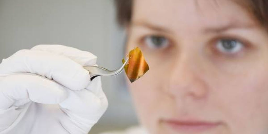
Quality Control in Silicon Wafer Manufacturing
Inspection Techniques
Quality testing in silicon wafer production is a laborious procedure that uses a variety of tools and methodologies to properly inspect each wafer. Adhering to industry standards and rigorous quality testing is more than a habit; it is a commitment to perfection.
Common Defects and Solutions
One of the primary challenges in silicon wafer manufacturing is maintaining the purity of the silicon throughout the manufacturing process. The electrical properties of silicon wafers, which are critical to their function in electronic devices, are highly sensitive to impurities. Even trace amounts of impurities can significantly alter these properties, leading to device failure.
Maintaining High Standards
- Cost-Efficiency: Identifying and correcting faults early in the production process is important for both quality and efficiency. Quality testing reduces the manufacture of faulty wafers, lowering material waste and production costs.
- Customer Satisfaction: Meeting or exceeding quality standards demonstrates a manufacturer’s dedication to excellence. Consistent delivery of high-quality silicon wafers builds customer trust, increases satisfaction, and creates long-term relationships.
Challenges and Future Trends
The silicon wafer manufacturing process is not without its challenges. High costs and energy consumption are significant hurdles that manufacturers must overcome. The production of silicon wafers requires substantial financial investment and energy resources, making it a costly endeavor.
High Costs and Energy Consumption
The silicon wafer manufacturing process is not without its challenges. High costs and energy consumption are significant hurdles that manufacturers must overcome. The production of silicon wafers requires substantial financial investment and energy resources, making it a costly endeavor.
Innovations in Manufacturing
To address these challenges, the industry is focusing on innovations in manufacturing. These include increasing wafer diameter, improving surface quality, and developing new crystal growth methods. Together, these trends in silicon wafer manufacturing aim to enhance efficiency and reduce costs.
Future Outlook for Silicon Wafers
Looking ahead, the future of silicon wafers appears promising. The continuous demand for faster, smaller, and more power-efficient devices drives ongoing advancements. Emerging technologies such as quantum computing and new materials like graphene are expected to play a crucial role in shaping the future of silicon wafer manufacturing.
Conclusion
This comprehensive guide has delved into the intricate world of silicon wafer manufacturing, from the initial extraction of silicon to the final stages of wafer polishing. By exploring each step in detail, we have highlighted the complexity and precision required in producing these essential components of modern electronics. Whether you are a student, a professional in the electronics industry, or simply someone with a keen interest in technology, this guide provides a thorough understanding of the processes that underpin the semiconductor industry. As we continue to advance technologically, the importance of mastering these manufacturing techniques cannot be overstated. We hope this guide has enriched your knowledge and appreciation of the fascinating journey from raw silicon to the sophisticated semiconductor wafers that power our everyday devices.
Frequently Asked Questions
What is a silicon wafer?
A silicon wafer is a thin slice of semiconductor material, typically silicon, which serves as the substrate for microelectronic devices. These wafers are essential components in the manufacturing of integrated circuits and other electronic devices.
How are silicon wafers made?
The manufacturing of silicon wafers involves several steps, including the extraction of silicon from quartz, purification, crystal growth (using methods such as the Czochralski process or Float Zone process), slicing the crystal into wafers, and polishing to achieve a smooth surface.
What is the Czochralski process?
The Czochralski process is a method of crystal growth used to obtain single crystals of semiconductors like silicon. In this process, a seed crystal is dipped into molten silicon and slowly pulled upwards while rotating, allowing a cylindrical crystal to form.
Why is doping important in silicon wafer manufacturing?
Doping is the process of adding impurities to silicon wafers to change their electrical properties. This is crucial for creating p-type or n-type semiconductors, which are essential for the functionality of electronic devices.
What role does photolithography play in silicon wafer manufacturing?
Photolithography is a process used to transfer patterns onto the silicon wafer. It involves coating the wafer with a light-sensitive material, exposing it to a pattern of light, and then developing the pattern. This is a critical step in creating the intricate circuits found in electronic devices.
What are the common defects in silicon wafers and how are they addressed?
Common defects in silicon wafers include dislocations, impurities, and surface irregularities. These defects are addressed through rigorous quality control measures, including inspection techniques and corrective processes like chemical-mechanical planarization (CMP) to ensure high-quality wafers.