Understanding Wafer Level Burn-In: A Comprehensive Guide
Wafer Level Burn-In (WLBI) represents a pivotal process in the semiconductor manufacturing industry. It involves subjecting integrated circuits and semiconductor devices to rigorous electrical testing while they are still in wafer form. This method is essential for detecting and screening out potential early-life device failures, thereby improving overall product yield and reliability. As technology advances, WLBI continues to evolve, offering new techniques and methods that enhance its effectiveness and efficiency. This comprehensive guide aims to delve into the fundamentals, technological advancements, implementation strategies, benefits, real-world applications, testing parameters, and comparisons with other testing methods of WLBI.
Key Takeaways
- Wafer Level Burn-In (WLBI) is crucial for identifying early-life failures in semiconductor devices, enhancing product reliability and yield.
- Technological advancements in WLBI are continuously improving the effectiveness and efficiency of the burn-in process.
- Implementing WLBI in quality control requires careful planning, overcoming challenges, and adhering to best practices.
- WLBI offers significant benefits, including improved reliability, cost efficiency, and enhanced product yield.
- Comparing WLBI with other testing methods highlights its unique advantages and industry adoption, making it a preferred choice in semiconductor manufacturing.
The Fundamentals of Wafer Level Burn-In
Definition and Importance
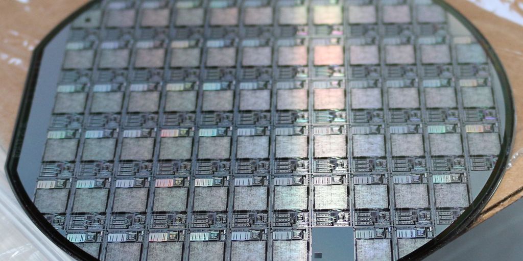
Wafer Level Burn-In (WBI) is a critical process in semiconductor manufacturing that involves subjecting integrated circuits to electrical testing while they are still in wafer form. This process is essential for detecting and screening out potential early life device failures. By identifying defects at this stage, manufacturers can ensure that only "known-good" RAM chips proceed to the next stages of production, thereby improving the overall product yield.
Key Components Involved
The WBI process typically utilizes conventional wafer probers and multi-chip probe card environments. These tools allow for the effective screening of reliability failures in random access memories on a wafer. The technology does not require any specialized equipment, making it a practical solution for many manufacturers. Key components include:
- Wafer probers
- Multi-chip probe cards
- Temperature and voltage control systems
Comparison with Die-Level Burn-In
Die-Level Burn-In (DLBI) approaches are also used in the industry, often involving temporary bare die carriers. While DLBI is effective, WBI offers several advantages. For instance, conducting burn-in in wafer form is more attractive to semiconductor manufacturers as it holds the promise of reducing the total cost to manufacture die, regardless of the packaging destination. Additionally, WBI can improve product yield by allowing for the replacement of failed components with spare rows or columns during the burn-in process.
Technological Advancements in Wafer Level Burn-In
New Techniques and Methods
Recent advancements in wafer level burn-in (WLBI) technology have introduced more efficient and reliable methods for screening semiconductor devices. One notable technique is the use of conventional wafer probers and multi-chip probe cards, which eliminate the need for additional specialized equipment. This approach not only simplifies the process but also enhances the accuracy of detecting potential failures in random access memories (RAM) before die-sorting.
Impact on Semiconductor Manufacturing
The integration of WLBI in semiconductor manufacturing has significantly reduced the overall cost of producing die. By conducting burn-in tests at the wafer level, manufacturers can identify and replace defective components early in the production cycle. This early detection leads to higher product yields and ensures that only "known-good" die proceed to the packaging stage. Additionally, the ability to perform burn-in tests on wafers, regardless of their packaging destination, offers greater flexibility and efficiency in the manufacturing process.
Future Trends
Looking ahead, the future of WLBI technology is promising, with ongoing research focused on further improving its efficiency and effectiveness. Emerging trends include the development of more advanced probe cards capable of handling higher densities and more complex semiconductor designs. Additionally, there is a growing interest in integrating artificial intelligence and machine learning algorithms to enhance the data analysis and interpretation of burn-in test results. These advancements are expected to further solidify WLBI’s role as a critical component in semiconductor manufacturing and quality control.
Implementing Wafer Level Burn-In in Quality Control
Steps for Effective Implementation
To effectively implement wafer level burn-in (WLBI) in quality control, follow these steps:
- Choose the most appropriate type of burn-in test for your specific semiconductor components.
- Design the burn-in test to expose components to high temperatures and voltage levels, ensuring they meet or exceed their rated operating conditions.
- Integrate the burn-in test into the overall quality control plan to identify and address specific quality control problems before products leave manufacturing facilities.
- Use conventional wafer probers and multi-chip probe card environments to streamline the process.
- Monitor and analyze the results to segregate potential early high failure rate populations and improve product yield.
Challenges and Solutions
Implementing WLBI comes with its own set of challenges. One major challenge is the potential for out-of-character performance indicators that may weaken properly functioning components. To address this, design the burn-in tests to trigger these indicators without compromising the integrity of the components. Another challenge is the need for specialized equipment, which can be mitigated by using conventional wafer probers and multi-chip probe card environments.
Best Practices
To ensure the success of WLBI in quality control, adhere to the following best practices:
- Regularly update the burn-in test parameters to reflect the latest technological advancements.
- Conduct periodic reviews of the burn-in test results to ensure they align with the overall quality control objectives.
- Train personnel on the importance of burn-in tests and how to effectively implement them.
- Maintain a detailed log of all burn-in tests conducted, including the conditions and results, to facilitate continuous improvement.
By following these steps and best practices, companies can significantly improve the reliability and quality of their semiconductor products.
Benefits of Wafer Level Burn-In
Improved Reliability
Wafer Level Burn-In (WLBI) significantly enhances the reliability of semiconductor devices. By subjecting integrated circuits to electrical testing while they are still in wafer form, potential early life device failures can be detected and screened out. This process ensures that only known-good chips proceed to the next stages of manufacturing, thereby improving the overall reliability of the final product.
Cost Efficiency
Implementing WLBI can lead to substantial cost savings for semiconductor manufacturers. The possibility of conducting burn-in in wafer form is more attractive and holds the promise of reducing the total cost to manufacture die, regardless of the packaging destination. This is a strong testimony of the advantage of wafer level burn-in as a better alternative to package part burn-in. By identifying and eliminating defective units early in the process, manufacturers can avoid the costs associated with packaging and testing faulty devices at later stages.
Enhanced Product Yield
WLBI technology effectively screens reliability failures of random access memories on a wafer, prior to die-sorting. As a result, obtaining “known-good” RAM chips becomes much more realistic. Since most of the failures occurred during the WBI can be replaced by spare rows or columns, the product yield improves. This leads to a higher number of functional chips per wafer, maximizing the efficiency and profitability of semiconductor manufacturing.
Case Studies and Real-World Applications
Success Stories
This collection of case studies delves deep into the pivotal role played by Smiths Interconnect in the semiconductor sector. Through real-world examples, we explore how companies have successfully implemented Wafer Level Burn-In (WLBI) to enhance product reliability and yield. One notable success story involves a major semiconductor manufacturer that reduced failure rates by 30% after integrating WLBI into their quality control process.
Lessons Learned
From these case studies, several key lessons emerge. First, the importance of a well-designed testing protocol cannot be overstated. Second, the integration of WLBI requires careful planning and execution to avoid potential pitfalls. Lastly, continuous monitoring and data analysis are crucial for ongoing success.
Industry Insights
Industry experts agree that WLBI is becoming increasingly vital in the semiconductor market. The advancements in WLBI technology have not only improved testing efficiency but also reduced costs. Companies that have adopted WLBI report higher customer satisfaction and fewer product recalls, underscoring its value in modern semiconductor manufacturing.
Wafer Level Burn-In Testing Parameters
Temperature and Voltage Levels
A burn-in test subjects a semiconductor to temperatures and voltage levels at or exceeding their rated operating conditions. This allows workers to identify and address specific quality control problems before products leave manufacturing facilities. Some burn-in tests examine other factors, such as component usage time. Whenever an operating condition has a specified upper limit, people can run burn-in tests to ensure their products meet or exceed specifications.
Duration of Tests
Those overseeing semiconductor production testing offer various answers when asked how long burn-in tests should take. Some suggest estimating how long and often people will use the devices containing these components and basing the test length on approximate metrics. Others have much more straightforward—but perhaps overly broad—suggestions, such as considering a burn-in test useful only if running it for at least a day.
Data Analysis and Interpretation
Wafer-level testing refers to a critical process of subjecting integrated circuits and semiconductor devices to electrical testing while they are still in wafer form. Burn-in is a temperature/bias reliability stress test used in detecting and screening out potential early life device failures. This hands-on approach ensures that the components meet the required specifications before they are integrated into larger systems.
Comparing Wafer Level Burn-In with Other Testing Methods
Advantages and Disadvantages
Wafer Level Burn-In (WLBI) offers several advantages over other testing methods. One of the primary benefits is the ability to test multiple devices simultaneously, which significantly reduces testing time and cost. Additionally, WLBI can identify potential early high failure rate populations, ensuring a statistically more reliable product population is delivered to the customer. However, it also has its disadvantages, such as the complexity of the setup and the need for specialized equipment.
Use Cases
WLBI is particularly useful in scenarios where high reliability is crucial, such as in aerospace and medical devices. It is also beneficial for application-specific deliverable components, as it can trigger out-of-character performance indicators without weakening properly functioning ones. This makes it an essential part of the quality control plan for many semiconductor manufacturers.
Industry Adoption
The adoption of WLBI varies across industries. In semiconductor manufacturing, it is often considered a "permission to play" credential, providing a pedigree certificate for convincing customers of the reliability assurance their products carry. While some industries have fully embraced WLBI, others still rely on conventional packaging and other testing methods. The choice often depends on the specific requirements and constraints of the industry.
Conclusion
Wafer Level Burn-In (WLBI) is an indispensable process in semiconductor manufacturing, providing a critical layer of reliability and quality assurance. By subjecting wafers to rigorous stress tests at elevated temperatures and voltages, manufacturers can identify and mitigate potential early-life failures, ensuring that only the most robust devices proceed to the next stages of production. This not only enhances the overall yield but also significantly reduces the cost and time associated with post-production testing. As the semiconductor industry continues to evolve, the implementation of WLBI will remain a cornerstone of quality control, driving advancements in technology and maintaining the high standards required for modern electronic devices.
Frequently Asked Questions
What is Wafer Level Burn-In (WLBI)?
Wafer Level Burn-In (WLBI) refers to the process of subjecting integrated circuits and semiconductor devices to electrical testing while they are still in wafer form. This helps in detecting and screening out potential early-life device failures.
How does WLBI differ from Die-Level Burn-In (DLBI)?
While WLBI tests the entire wafer, DLBI involves testing individual dies after they have been separated from the wafer. WLBI is generally more cost-effective and can improve product yield by identifying failures earlier in the manufacturing process.
What are the main benefits of implementing WLBI?
The main benefits of WLBI include improved reliability, cost efficiency, and enhanced product yield. It allows for early detection of defects, reducing the chances of field failures and increasing the overall quality of the semiconductor devices.
What technological advancements have been made in WLBI?
Recent advancements in WLBI include new techniques and methods that enhance the effectiveness of the burn-in process. These advancements have a significant impact on semiconductor manufacturing, making the process more efficient and reliable.
What parameters are crucial for WLBI testing?
Key parameters for WLBI testing include temperature and voltage levels, the duration of the tests, and the methods used for data analysis and interpretation. These factors are critical in ensuring the effectiveness of the burn-in process.
What challenges are associated with implementing WLBI?
Challenges in implementing WLBI include the need for specialized equipment, potential yield loss due to over-stressing devices, and the complexity of integrating WLBI into existing manufacturing processes. However, these challenges can be mitigated with proper planning and best practices.