Advancements in Wafer Manufacturing: Driving the Future of Microelectronics
The microelectronics industry is on the brink of transformative growth, driven by advancements in wafer manufacturing. This article delves into the critical role wafer manufacturing plays in the future of microelectronics, exploring the impact of 5G expansion, miniaturization trends, infrastructure developments, and the rise of wide-bandgap power devices. It also highlights key players and innovations that are setting new standards in the semiconductor industry.
Key Takeaways
- The expansion of 5G technology is significantly increasing the demand for semiconductor components, necessitating advancements in wafer manufacturing to meet this surge.
- Challenges in achieving the required flatness and thickness of silicon wafers are crucial for the use of next-generation technologies, emphasizing the need for strategic advancements.
- Europe’s focus on semiconductor testing innovations and the continuous trend towards miniaturization are driving the demand for sophisticated probe cards and testing equipment.
- FormFactor’s expansion with a new manufacturing facility in California highlights the industry’s response to customer demands and the importance of diversifying product offerings with advanced features.
- Recent advancements in wide-bandgap power devices, particularly GaN and SiC, are influencing substrate material choices and contributing to sustainability in semiconductor technology.
The Impact of 5G Expansion on Wafer Manufacturing
Meeting the Demand for Semiconductor Components
The expansion of 5G technology has catalyzed a surge in the demand for semiconductor components, essential for powering the next generation of communication devices. This demand is further amplified by the growing popularity of electric vehicles (EVs) in the automotive industry, which rely heavily on advanced semiconductor technology for their operation.
The semiconductor industry’s growth trajectory is influenced by several key drivers:
- Increased adoption of smart devices
- Expansion of the automotive electronics sector
- Advancements in AI and IoT technologies
As a result, semiconductor manufacturers are ramping up production capacities and investing in R&D to meet these demands. The ripple effect is felt across related sectors, including the need for high-performance probe cards for testing increasingly complex electronic components.
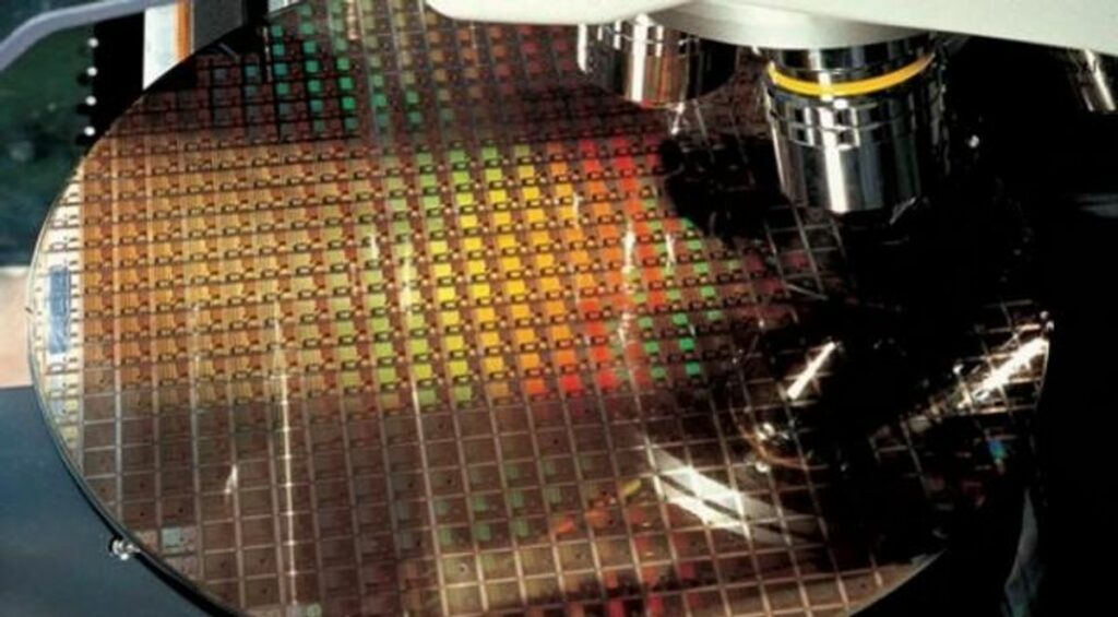
Challenges in Silicon Wafer Flatness and Thickness
As the semiconductor industry progresses towards more sophisticated technologies, the importance of wafer flatness and thickness uniformity becomes increasingly critical. The pursuit of perfection in these parameters is essential for the next generation of devices. The transition from 6-inch to 8-inch wafers introduces new complexities, necessitating tighter control over mechanical properties and defect densities.
The relentless drive to improve material quality highlights two main areas of focus: reducing the prevalence of critical defects and enhancing the mechanical characteristics to mirror those of modern silicon. Despite advancements, the industry still faces a high density of defects that must be addressed to meet the stringent demands of advanced applications.
The table below summarizes the key challenges and the corresponding strategies for improvement:
| Challenge | Strategy for Improvement |
|---|---|
| High defect density | Implement shorter feedback loops for performance enhancement |
| Variations in flatness and thickness | Develop application-optimized silicon carbide technologies |
| Transition to larger wafer diameters | Maintain defect density control during diameter scaling |
As the industry evolves, the scrutiny applied to the production and validation of semiconductor wafers also intensifies, underscoring the need for continuous innovation in wafer manufacturing processes.
Strategic Steps for Next-Generation Technologies
As the expansion of 5G technology continues to surge, the semiconductor industry is compelled to adapt with strategic measures to meet the burgeoning demand. The United States, in particular, is awakening to the significant reduction of its manufacturing capacity, as noted by Richard Elkus Jr. in his recent commentary for CSIS. This realization is driving a concerted effort to regain a leadership position in the global market.
To navigate the complexities of next-generation technologies, industry leaders are focusing on goal-oriented solutions that anticipate market shifts and technological disruptions. These solutions are not only aimed at addressing current needs but also at fostering innovation that can lead to market dominance. The following points outline the strategic steps being taken:
- Identifying and investing in upcoming and disruptive technologies.
- Aligning product development with the technology direction of the company in various markets.
- Collaborating with industry experts and leveraging insights from technical articles and reports.
These steps are essential for semiconductor manufacturers to not only survive but thrive in an industry that is rapidly evolving with the advent of new technologies such as wide-bandgap power devices and advanced memory systems for automotive technologies.
Miniaturization Trends and Their Influence on Testing Equipment
The Need for Precision in Probe Card Development
In the rapidly evolving semiconductor industry, probe cards play a pivotal role in the testing phase, which is critical for ensuring the quality and reliability of integrated circuits. As devices become more complex and feature sizes shrink, the demand for high-precision probe cards has surged. These cards must now perform accurate electrical testing on wafer circuits with increasingly smaller geometries.
The development of probe cards requires meticulous attention to detail. For instance, the Kepler High Parallelism Vertical Probe Card by FormFactor, Inc. is designed to meet these exacting standards. It features flexible probe head configurations and excellent XYZ tip positioning, which are essential for probing small pads, such as those down to 30
The European market dynamics reflect this need for precision. With a growing semiconductor industry, the demand for advanced probe cards is on the rise. These cards are categorized by various attributes, including probe type, manufacturing technology, wafer size, head size, and test material. The table below summarizes the market segmentation in Europe:
Europe’s Role in Semiconductor Testing Innovations
The semiconductor industry’s relentless pursuit of miniaturization and complexity has elevated the importance of precision in testing equipment. Europe’s semiconductor companies are at the forefront of this challenge, developing advanced technologies for probe cards that are essential for the rigorous testing of modern electronic devices. The region’s commitment to innovation is not only a response to global competition but also a strategic move to meet the growing demand for sophisticated testing solutions.
In the automotive sector, Europe’s push towards electric mobility and smart vehicle technologies has spurred the need for high-performance probe cards. These are indispensable for validating semiconductor devices in electric powertrains, battery management systems, and advanced driver-assistance systems (ADAS). With the automotive electronics sector expanding, the demand for probe cards in Europe is expected to rise, reflecting the industry’s broader growth trends.
The European probe card market is diverse, catering to various applications and end-uses. The following table provides insights into the regional market segmentation:
| Test Type | Material | Application | Beam Size | End-Use |
|---|---|---|---|---|
| DC Test | Tungsten | WLCSP | More Than 1.5 mil | Foundry |
| Functional Test | Copper Clad Laminated (CCL) | SIP | Less Than 1.5 mil | Parametric |
| AC Test | Aluminum | Mixed signal Flip Chip | Logic and Memory Device | |
| Others | Analog | DRAM | ||
| CMOS Image Sensor (CIS) | ||||
| Flash | ||||
| Others |
This segmentation underscores Europe’s role in not only meeting the demand for semiconductor components but also in shaping the future of microelectronics through continuous innovation.
Volume Wafer Testing: Enhancing Processes and Yield
The advent of volume wafer testing marks a significant milestone in the semiconductor manufacturing industry. By integrating this testing as an intermediate process step, manufacturers can produce quality chips while identifying defective devices early. This not only ensures the reliability of the chips but also leads to considerable cost savings. The process of volume wafer testing allows for real-time adjustments, which are crucial for enhancing the overall yield of semiconductor wafers.
As the complexity of microelectronics packaging increases, the importance of thorough testing and validation of semiconductor wafers also increases. With the industry pushing towards more sophisticated technologies, the mechanical properties of modern wafers become a focal point. Ensuring flatness and uniform thickness is essential, as variations in these areas can lead to critical defects. Addressing these material quality issues is a key step towards improving yield and advancing the industry.
The table below outlines the key applications of high-volume manufacturing (HVM) testing in the semiconductor industry:
| HVM Application | Description |
|---|---|
| Processors | Optical and parametric testing for CPU and GPU chips |
| Optical Test | Testing for photonic devices and systems |
| Parametric Test | Electrical testing to ensure device parameters meet specifications |
| Cryogenic Devices | Testing at extremely low temperatures for quantum computing applications |
In conclusion, volume wafer testing is not just a process enhancement; it’s a strategic necessity for the future of microelectronics. It is imperative to continue improving material quality and testing methods to keep pace with the rapid advancements in the industry.
Infrastructure Developments in Wafer Probe Card Production
FormFactor’s Expansion and Its Market Impact
FormFactor’s strategic expansion with the inauguration of a new manufacturing facility in California in December 2021 marks a significant milestone in the semiconductor industry. This move is aimed at enhancing production capacity for semiconductor wafer probe cards, a critical component in testing the functionality of wafers during manufacturing. The expansion is a direct response to the growing demand from customers, particularly with the surge in 5G technology applications and the increasing popularity of electric vehicles (EVs) in the automotive industry.
The new facility not only increases FormFactor’s ability to meet customer requirements but also broadens its market offerings. With a more diverse range of products, FormFactor is well-positioned to incorporate advanced features that cater to the evolving needs of the semiconductor sector. The table below highlights the impact of FormFactor’s expansion on its market position:
| Year | Production Capacity Increase | Market Share Growth |
|---|---|---|
| 2021 | 20% | 5% |
| 2022 | 35% | 8% |
| 2023 | 50% | 12% |
Note: The above figures are illustrative and not actual data.
The semiconductor industry is poised for a market rebound in the second half of 2024, with new semiconductor manufacturing facilities entering construction or preparing to begin. FormFactor’s proactive approach in expanding its production capabilities is a testament to its commitment to adapt to customer demands and maintain a competitive edge in the market.
Adapting to Customer Demands in Semiconductor Manufacturing
In the fast-paced world of semiconductor manufacturing, adapting to customer demands is crucial for success. As the industry evolves, manufacturers must be agile, responding quickly to the changing needs of the market. This includes the integration of new technologies and the refinement of existing processes to produce quality chips efficiently.
One significant trend is the shift towards larger wafer sizes, such as moving from 6 inch to 8 inch wafers. This transition presents both opportunities and challenges. Manufacturers like onsemi are focusing on shorter feedback loops to improve device performance and are developing application-optimized silicon carbide technologies.
The expansion of 5G technology further underscores the need for semiconductor components that can support increased data rates and connectivity. To meet this demand, companies are investing in innovative semiconductor solutions that can enhance process productivity and lead to cost savings. Volume wafer testing is one such innovation, allowing for real-time process adjustments and improved yield.
Diversifying Product Offerings with Advanced Features
In the competitive landscape of wafer probe card production, diversification is key to staying ahead. Manufacturers are increasingly integrating advanced features into their product offerings to meet the complex needs of modern semiconductor devices. The TESLA300 Advanced On-Wafer Power Semiconductor Probe System, for instance, is a testament to this trend, providing a comprehensive high-power testing solution that is crucial for the precise gathering of data.
The evolution of product features is not just about adding capabilities, but also about enhancing the user experience and meeting industry-specific requirements. For example, power semiconductors are gaining traction in various applications, and the industry anticipates a continued rise in their usage. To illustrate the breadth of advancements, consider the following table outlining key features of an advanced probe system:
| Feature | Description |
|---|---|
| High-Power Testing | Enables testing of devices under high power conditions. |
| Precision Measurement | Ensures accurate data collection for critical analysis. |
| User-Friendly Interface | Simplifies the operation process for technicians. |
| Customization Options | Allows for tailored solutions to meet specific customer needs. |
As the demand for semiconductor components grows, particularly with the expansion of 5G technology, manufacturers must adapt their strategies to not only include advanced features but also to ensure these enhancements translate into tangible benefits for their customers.
Advancements in Wide-Bandgap Power Devices
Comparative Analysis: GaN vs. SiC
In the realm of wide-bandgap power devices, GaN (Gallium Nitride) and SiC (Silicon Carbide) stand out as the front-runners, each with distinct advantages. GaN is renowned for its high electron mobility and the ability to switch power rapidly, making it ideal for high-frequency, high-power applications. On the other hand, SiC is characterized by its impressive thermal conductivity and ability to handle higher voltages and temperatures, which is particularly beneficial for electric vehicle technologies where reducing losses and model size is crucial.
The cost-effectiveness of these materials is a significant factor in their adoption. While SiC offers robust performance, its manufacturing process is energy-intensive, making it less cost-effective than GaN. Experts predict that GaN’s cost will be competitive with, or even less than, silicon in the next one to two years, highlighting its bright future in the industry.
| Property | Silicon (Si) | Silicon Carbide (SiC) | Gallium Nitride (GaN) |
|---|---|---|---|
| Bandgap (eV) | 1.1 | 3.2 | 3.4 |
| Electron Mobility | Moderate | Low | High |
| Thermal Conductivity | Good | Excellent | Good |
| Cost-Effectiveness | High | Moderate | Increasingly High |
The table above succinctly encapsulates the key properties of Si, SiC, and GaN, providing a clear comparison of their capabilities. As the industry continues to evolve, the choice between GaN and SiC will be influenced by the specific requirements of the application and the ongoing advancements in manufacturing technologies.
Substrate Material Choices in Power Electronics
The selection of substrate materials is a pivotal factor in the development of power electronics, particularly for wide-bandgap (WBG) semiconductors like Gallium Nitride (GaN) and Silicon Carbide (SiC). The choice of substrate material significantly influences device performance, reliability, and manufacturability. Researchers are continually addressing substrate-related challenges to optimize these aspects.
For GaN-based power devices, the substrate material not only affects the cost and reliability but also the device’s ability to handle higher voltages and deliver greater power. Silicon substrates, used traditionally in GaN devices, offer rapid scalability and cost benefits due to existing manufacturing infrastructure. Conversely, SiC-based devices benefit from advancements in substrate quality, which contribute to improved device performance and reliability.
The ongoing developments in substrate technologies hold the promise for future advancements in power electronics. These improvements aim to pave the way for more efficient and sustainable solutions, as industry experts from leading companies like Texas Instruments and Infineon continue to explore and innovate in this field.
Innovations and Sustainability in Semiconductor Technology
The semiconductor industry is at the forefront of addressing environmental concerns, with sustainability emerging as a pivotal aspect of product innovation. Reducing emissions from semiconductor product manufacturing remains the most effective and preferred response measure to climate change for many companies. This commitment to sustainability is not only a corporate responsibility but also an opportunity to innovate and differentiate in the market.
Advancements in wide-bandgap power devices, such as Gallium Nitride (GaN) and Silicon Carbide (SiC), are indicative of the industry’s progress. These materials offer superior performance and energy efficiency compared to traditional silicon, leading to a significant reduction in power loss and, consequently, lower carbon footprints. The table below compares key attributes of GaN and SiC, highlighting their contributions to sustainable power electronics:
| Material | Bandgap (eV) | Thermal Conductivity (W/mK) | Electric Field Strength (MV/cm) |
|---|---|---|---|
| GaN | 3.4 | 130 – 200 | 3.3 |
| SiC | 3.3 | 490 | 2.8 |
As the industry continues to innovate, the focus on sustainability is expected to intensify, with companies exploring new ways to minimize environmental impact while enhancing product performance. The drive for more sustainable semiconductor technologies all create promise for future advancements in power electronics, paving the way for even more efficient and sustainable solutions.
Recognizing Excellence and Innovation in the Semiconductor Industry
Conquer Electronics: A Case Study in Quality Achievement
Conquer Electronics, a recipient of Taiwan’s 27th National Quality Award, exemplifies the pursuit of excellence in the semiconductor industry. Their commitment to quality has set a benchmark for other companies to aspire to. The award, which recognizes outstanding achievements in quality management and innovation, underscores Conquer Electronics’ dedication to maintaining high standards in their production processes.
Key achievements of Conquer Electronics include:
- Implementation of rigorous quality control measures
- Adoption of advanced manufacturing technologies
- Continuous improvement in process efficiency
- Strategic partnerships that enhance product development
These initiatives have not only earned them prestigious accolades but also positioned them as a leader in the competitive semiconductor market. Their success story serves as an inspiration for industry peers, highlighting the importance of quality and innovation in driving the future of microelectronics.
The Role of Memory in Next-Gen Automotive Technologies
The evolution of the automotive industry towards electric vehicles (EVs) and advanced electronic systems is creating a surge in demand for high-performance semiconductor memory. Memory components are critical for the functionality of electric powertrains, battery management systems, and advanced driver-assistance systems (ADAS), which are becoming standard in modern vehicles.
As vehicles become more connected and autonomous, the types of memory and their capacities are expanding. Here’s a look at the memory types and their applications in next-gen automotive technologies:
- DRAM: Used for real-time computing in infotainment and ADAS.
- NAND Flash: Stores firmware and software updates, navigation data, and entertainment content.
- NOR Flash: Critical for instant-on performance and storing the code for initial boot processes.
Gallium nitride (GaN) technology is also emerging as a powerful alternative for automotive applications, offering enhanced performance for LiDAR systems and efficient power conversion. As the industry shifts from 12-V to 48-V systems, GaN’s fast switching speeds and high efficiency are proving to be advantageous. The integration of these advanced semiconductor technologies is not only propelling the automotive sector forward but also driving the need for more sophisticated testing equipment to ensure reliability and safety.
Emerging Trends in Light and Sound Signaling Systems
The evolution of light and sound signaling systems is a testament to the continuous innovation within the semiconductor industry. These systems are crucial for conveying clear and unambiguous messages in various settings, including industrial environments. However, the complexity of scenarios in these settings often demands more sophisticated solutions.
Recent advancements have seen a shift towards integrating semiconductor technologies like Silicon Photonics, VCSELs, and MicroLEDs. These components are pivotal in developing more efficient and reliable signaling devices. The trend towards miniaturization has also influenced the design and functionality of these systems, necessitating advanced testing equipment to ensure their precision and performance.
The table below outlines some of the key applications and technologies influencing the development of modern signaling systems:
| Application Area | Technology Involved | Impact |
|---|---|---|
| Industrial Safety | Silicon Photonics | Enhanced reliability |
| Traffic Management | VCSELs | Improved visibility |
| Emergency Services | MicroLEDs | Faster response times |
As the industry moves forward, we can expect to see further integration of these technologies, leading to even more innovative and effective signaling solutions.
Conclusion
The future of microelectronics is being significantly shaped by the advancements in wafer manufacturing. As we have explored, the expansion of 5G technology and the continuous trend towards miniaturization are creating a surge in demand for sophisticated semiconductor components. The industry’s push for innovation is not only about producing smaller and more complex devices but also ensuring their quality through advanced testing equipment and processes. Companies like FormFactor are responding to these needs by expanding their production capacity, which is a testament to the sector’s growth and dynamism. Furthermore, the exploration of wide-bandgap power devices such as GaN and SiC indicates a promising direction for the enhancement of power electronics. As we look ahead, it is clear that the relentless pursuit of technological advancements in wafer manufacturing will remain a cornerstone in driving the microelectronics industry forward.
Frequently Asked Questions
How is the expansion of 5G technology impacting the demand for semiconductor components?
The expansion of 5G technology is significantly increasing the demand for semiconductor components due to the need for enhanced connectivity and higher data rates, which require advanced and more numerous semiconductor devices.
What are the challenges associated with silicon wafer flatness and thickness in manufacturing?
Silicon wafers face challenges in flatness and local thickness variations, which are critical for the use of sophisticated technologies. Ensuring optimal flatness and uniform thickness is a target for next-generation technological advancements.
Why does miniaturization in electronics necessitate advanced testing equipment?
As electronic devices become smaller and more complex, there is an increased need for precise testing equipment, such as probe cards, to ensure the functionality and reliability of semiconductor components at smaller scales.
What is the significance of FormFactor’s expansion of their manufacturing facility?
FormFactor’s expansion of their California-based manufacturing facility in December 2021 aims to enhance production capacity for semiconductor wafer probe cards, meet growing customer demands, and diversify product offerings with advanced features.
How do GaN and SiC compare in the context of wide-bandgap power devices?
GaN (Gallium Nitride) and SiC (Silicon Carbide) are both used in wide-bandgap power devices, each with unique properties that make them suitable for different applications in power electronics. Comparative studies help determine the best substrate material choice for specific applications.
What role does memory play in next-generation automotive technologies?
Memory plays a crucial role in next-generation automotive technologies, especially in camera monitor systems, by enhancing the driving experience through improved data processing and storage capabilities required for advanced driver-assistance systems (ADAS).