Exploring the Dynamics of Wafer Growth: How the Semiconductor Market is Scaling New Heights
The semiconductor industry is experiencing a period of rapid innovation and growth, driven by advancements in wafer growth and fabrication technologies. As the demand for smaller, more powerful electronic devices continues to rise, the need for high-precision manufacturing processes has never been greater. This article delves into the dynamics of wafer growth, exploring the evolution of measurement in wafer fabrication, advancements in process window modeling, innovations in power delivery and defect management, next-generation deposition technologies, and the fostering of innovation and trends within the industry.
Key Takeaways
- Hendrik Hans emphasizes the importance of vertical scaling and the role of Lam’s Metior in surpassing the limitations of optical measurement in wafer fabrication.
- QingPeng Wang’s work on virtual fabrication illustrates its significance in DRAM capacitor patterning and the evaluation of process windows, as well as its impact on advanced 3D NAND structures.
- Innovations in backside wafer processing by Sandy Wen and James Kim’s techniques for correcting asymmetric wafer map defects highlight the progress in power delivery and defect management.
- Aaron Fellis introduces SPARC technology and the role of atomic layer deposition by Lam Research in advancing logic and DRAM, while Allison Parker discusses the yield improvements brought by bevel deposition solutions.
- Lam Capital’s support for semiconductor startups and the insights shared at SEMICON West 2022 by Lam Research indicate a strong commitment to fostering innovation and setting future industry trends.
The Evolution of Measurement in Wafer Fabrication
Hendrik Hans’ Insights on Vertical Scaling
In the realm of semiconductor manufacturing, vertical scaling has become a pivotal strategy for companies aiming to enhance integration and performance. Hendrik Hans highlights the significance of this approach, particularly in the context of mass metrology applications. Lam’s Metior technology has emerged as a game-changer, successfully addressing the limitations of traditional optical measurement techniques in the vertical scaling process.
The evolution of measurement tools is critical to maintaining the precision required for advanced functional materials. As feature sizes shrink and process variability increases, the industry faces the challenge of maintaining tight process windows. Hans’ insights suggest that innovative strategies, such as those employed by Metior, are essential for overcoming these hurdles and ensuring the preservation of cell positioning and shape, which are crucial for the modulation of cell fate in semiconductor materials.
The table below outlines the key benefits of vertical scaling in mass metrology:
| Benefit | Description |
|---|---|
| Enhanced Precision | Allows for more accurate measurements of smaller features. |
| Reduced Variability | Minimizes process step variability, ensuring consistent quality. |
| Improved Integration | Facilitates the integration of various processes and materials. |
As the industry continues to push the boundaries of miniaturization, the insights provided by experts like Hendrik Hans will be instrumental in guiding the future of wafer fabrication and semiconductor innovation.
The Role of Metior in Overcoming Optical Measurement Limitations
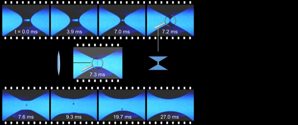
Semiconductor manufacturers are scaling new heights with vertical integration. Lam’s Metior succeeds where optical measuring falls short. Metior measures mass changes with a precision of 30 µg, equivalent to a change of 1.8Å for a silicon layer on a 300mm wafer. The advantages of Metior mass measurement technology are evident in its ability to provide accurate and reliable data for optimizing wafer growth processes.
Mass Metrology and Its Impact on Process Variability
In the pursuit of perfection within semiconductor manufacturing, mass metrology has emerged as a critical tool for ensuring consistency across the myriad of process steps. As devices scale down, the margin for error shrinks, making the role of mass metrology more significant than ever. This precision measurement technique is pivotal in identifying and controlling process variability, which can lead to defects and yield loss.
The manufacturing of a semiconductor chip is a complex dance of numerous process steps, each with potential for imperfections and variability. Mass metrology provides a quantitative approach to monitor and manage these variations, ensuring alignment with design specifications. By integrating mass metrology into the fabrication process, manufacturers can detect issues early and adjust processes accordingly, thereby enhancing the overall yield and reliability of semiconductor devices.
Here are some key benefits of mass metrology in semiconductor fabrication:
- Enhanced process control: Real-time data allows for immediate adjustments.
- Reduced variability: Consistent measurements lead to uniformity across wafers.
- Improved yield: Early detection of deviations helps prevent scrap and rework.
- Cost savings: Minimizing defects and variability translates to lower production costs.
Advancements in Process Window Modeling
QingPeng Wang’s Approach to DRAM Capacitor Patterning
QingPeng Wang, a Senior Semiconductor Process & Integration Engineer at Coventor, has been at the forefront of DRAM capacitor patterning, a critical aspect of memory design and fabrication. His work emphasizes the importance of process window modeling in the face of ever-narrowing windows due to device scaling. With smaller feature sizes, the margin for error shrinks, making precise patterning more crucial than ever.
Wang’s approach utilizes virtual fabrication to evaluate and optimize the DRAM capacitor patterning process. This technique allows for sensitivity analysis, which is instrumental in guiding inline process specifications and control. The table below summarizes the key benefits of using virtual fabrication in DRAM capacitor patterning:
| Benefit | Description |
|---|---|
| Enhanced Accuracy | Enables precise modeling of complex structures. |
| Process Optimization | Identifies optimal process parameters for patterning. |
| Risk Mitigation | Reduces the likelihood of defects and process variability. |
| Cost Efficiency | Lowers development costs by minimizing physical trial and error. |
By integrating virtual fabrication into the patterning process, Wang’s methodology not only improves the accuracy of DRAM capacitors but also contributes to the overall reliability and performance of memory devices.
The Significance of Virtual Fabrication in Process Evaluation
The advent of virtual fabrication has revolutionized the semiconductor industry, offering a powerful tool for engineers to simulate and optimize manufacturing processes before physical production begins. This technique is particularly valuable in the face of ever-narrowing process windows, where the margin for error is increasingly slim.
Virtual fabrication platforms, like Lam’s SEMulator3D, enable the exploration of various process scenarios. By creating a digital twin of the manufacturing process, engineers can predict the outcome of different patterning techniques, materials, and process sequences. This preemptive analysis is crucial for improving device performance and yield, especially in complex structures such as DRAM saddle fin profiles.
The benefits of virtual fabrication extend beyond process optimization. Training programs, such as the one initiated by Lam to educate up to 60,000 engineers in India, demonstrate the platform’s role in enhancing engineering education. By familiarizing the workforce with cutting-edge technology, the industry ensures a steady stream of skilled professionals adept at navigating the intricacies of semiconductor fabrication.
Channel Hole Profiles and Their Influence on 3D NAND Structures
The intricacies of channel hole profiles are critical to the performance and reliability of 3D NAND flash memory. As the industry pushes for higher density storage, the uniformity and precision of these microscopic structures become paramount. QingPeng Wang, a Senior Semiconductor Process & Integration Engineer, emphasizes the use of virtual fabrication as a tool for sensitivity analysis, which aids in maintaining stringent inline process specifications.
A recent advancement in the field is the development of a smart electrical screening methodology. This technique has shown promising results in the experimental phase, efficiently detecting and screening out defects without unexpected side effects. The table below summarizes the key findings from the study:
| Metric | Before Implementation | After Implementation |
|---|---|---|
| Defect Detection Rate | 85% | 98% |
| False Positive Rate | 20% | 5% |
| Throughput Impact | Moderate | Minimal |
These improvements are not just about enhancing current capabilities but also about setting the stage for future innovations in NAND technology. As we scale to new heights, the semiconductor market continues to evolve, with process control and defect management playing pivotal roles.
Innovations in Power Delivery and Defect Management
Sandy Wen’s Perspective on Backside Wafer Processing
Sandy Wen, a seasoned process integration engineer, has shed light on the once-overlooked aspect of semiconductor manufacturing: the backside of the wafer. The backside processing, particularly for power delivery, has become a critical area of focus as the industry strives for greater efficiency and performance.
In the past, the backside was often a source of complications, with incidents such as wafers detaching from robot blades during handling. However, with advancements in technology and a deeper understanding of backside dynamics, engineers like Wen are pioneering new methods to harness its potential.
- Improved handling techniques to prevent wafer loss
- Enhanced power delivery systems for better chip performance
- Innovative materials and processes to optimize backside integration
These developments not only enhance the reliability of semiconductor devices but also open up new avenues for chip design and functionality.
James Kim’s Techniques for Correcting Asymmetric Wafer Map Defects
Following James Kim’s exploration of asymmetric wafer map defects, the semiconductor industry is witnessing the rise of Coronus DX, a groundbreaking technology in 3D chipmaking. Coronus DX is revolutionizing the way engineers manage power delivery and defect correction by providing advanced tools for backside wafer processing and defect management.
The technology’s key features include:
- Enhanced defect detection algorithms that pinpoint inaccuracies with unprecedented precision.
- Innovative power routing techniques that optimize the distribution of power across complex 3D structures.
- A suite of diagnostic and repair tools that ensure the highest quality of wafer output.
Coronus DX’s impact on the semiconductor market is significant, offering manufacturers the ability to scale new heights in chip performance and reliability. As the industry continues to evolve, the adoption of such technologies will be crucial in maintaining a competitive edge in an increasingly demanding marketplace.
The Emergence of Coronus DX in 3D Chipmaking
The semiconductor industry is witnessing a significant leap forward with the introduction of Coronus DX, a pioneering bevel deposition solution tailored for 3D chipmaking. This innovation is poised to address some of the most pressing manufacturing challenges, leading to a substantial improvement in wafer yield. Coronus DX builds on Lam’s extensive history of innovation, particularly in bevel solutions, marking a new era in semiconductor fabrication.
The importance of Coronus DX can be further understood by considering the evolving landscape of 3D chip architectures. As devices become smaller and more powerful, the need for efficient 3D structures like DRAM and NAND is escalating. Coronus DX offers a unique technology that simplifies the production process while reducing costs, which is crucial for the industry’s advancement.
Here’s a glimpse at how Coronus DX stands to revolutionize 3D chipmaking:
- It provides a solution optimized for the complex geometries of 3D structures.
- The technology ensures higher consistency and quality in wafer production.
- By improving yield, it contributes to the cost-effectiveness of high-volume manufacturing.
Next-Generation Deposition Technologies and Their Applications
Aaron Fellis on the Advent of SPARC Technology
Aaron Fellis, Corporate VP and GM at Lam Research, has been at the forefront of developing SPARC technology, a groundbreaking approach to dielectric atomic layer deposition (ALD). Introduced on June 16, 2022, SPARC stands as a testament to Lam Research’s commitment to innovation in the semiconductor space, particularly for advanced logic and DRAM applications.
SPARC’s introduction is a pivotal moment for the industry, as it promises to enhance the capabilities of chips that are integral to a wide array of technologies, from mobile phones to cloud servers. The technology is designed to meet the ever-increasing demands for faster, smarter, and more efficient computing power.
The following are key benefits of SPARC technology:
- Enhanced film quality and uniformity
- Improved electrical performance
- Greater scalability for future technology nodes
- Compatibility with existing manufacturing processes
The Role of Atomic Layer Deposition in Advanced Logic and DRAM
Atomic Layer Deposition (ALD) has become a cornerstone technology in the semiconductor industry, particularly for advanced logic and DRAM applications. The precision and uniformity of ALD are pivotal in creating the thin films necessary for the ever-shrinking features of modern chips. As devices scale down in size, the management of surface roughness becomes increasingly critical, and ALD’s self-limiting surface reaction process addresses this by producing uniform coatings.
The integration of ALD in DRAM manufacturing is evident in the evolution of bit-line spacer integration schemes. With the miniaturization of DRAM cells, maintaining sensing margins and refresh times is a growing challenge. ALD technology facilitates the creation of spacers with the necessary precision, directly impacting the performance and reliability of memory chips.
As the market transitions from DDR4 to DDR5 and beyond, the role of ALD will only expand. The following table outlines the progression of mainstream memory technologies and their expected market adoption:
| Memory Technology | Current Mainstream | Expected Transition Period |
|---|---|---|
| DDR4 | Yes | 2021-2023 |
| LPDDR4 | Yes | 2021-2023 |
| DDR5 | Emerging | 2023-2025 |
| LPDDR5 | Emerging | 2023-2025 |
In conclusion, ALD is not just a method for thin film deposition; it is a critical enabler for the next generation of semiconductor devices. Its application in advanced logic and DRAM underscores its importance in meeting the demands of an industry that is constantly pushing the boundaries of miniaturization and performance.
Bevel Deposition Solutions and Their Yield Improvements
The introduction of Coronus DX marks a significant milestone in the realm of bevel deposition, particularly for 3D chipmaking. This innovative solution addresses critical manufacturing challenges and is poised to substantially enhance wafer yield. Building upon Lam’s extensive 15-year legacy in bevel technology, Coronus DX represents a leap forward in tackling the complexities of semiconductor fabrication.
Bevel deposition plays a crucial role in ensuring the integrity and performance of semiconductor devices. The process involves the precise application of materials on the wafer’s edge, which is critical for preventing defects that can arise during subsequent manufacturing steps. The following table summarizes the key benefits of implementing Coronus DX in the production line:
| Benefit | Description |
|---|---|
| Yield Improvement | Significantly reduces defectivity at the wafer edge, leading to higher overall yield. |
| Process Efficiency | Streamlines the deposition process, minimizing downtime and maintenance. |
| Cost Effectiveness | Lowers operational costs by improving material utilization and reducing waste. |
Lam’s commitment to innovation is further exemplified by their collaborative approach, as seen in their Spare Parts Program. This initiative, which fosters close collaboration with customers, has been instrumental in achieving rapid and predictable cost efficiency. The synergy between Lam’s technological advancements and customer-centric strategies underscores the company’s role in propelling the semiconductor industry forward.
Fostering Innovation and Trends in the Semiconductor Industry
Lam Capital’s Support for Semiconductor Startups
Lam Capital, the investment arm of Lam Research, plays a pivotal role in nurturing the next generation of semiconductor innovations. Through initiatives like the Lam Capital Venture Competition, startups in the semiconductor space are provided with not only crucial funding but also the exposure they need to thrive in a competitive market. This unique contest underscores Lam’s commitment to fostering innovation and growth within the industry.
In addition to financial support, Lam Capital offers startups access to a wealth of industry knowledge and resources. The SEMICON West 2022 conference, for instance, served as a platform where Lam Research shared insights on future technologies and industry trends, further contributing to the dialogue that shapes the semiconductor landscape. The CHIPS and Science Act signing ceremony, attended by Lam Research CEO Tim Archer, highlights the company’s active participation in policy-making and industry advancement.
Lam’s expansion of R&D operations, including new technology centers and manufacturing sites, indicates a broader strategy to support the semiconductor ecosystem. This expansion not only benefits Lam’s internal capabilities but also provides a richer environment for startups to collaborate and innovate.
SEMICON West 2022: A Platform for Future Technologies
SEMICON West 2022 served as a pivotal gathering for industry leaders and innovators, where Lam Research and others from the electronics supply chain engaged in meaningful dialogues. The event highlighted the trajectory of semiconductor technologies, showcasing advancements and setting the stage for future developments.
The conference was not just a showcase but also a forum for strategic insights. Participants had the opportunity to attend various talks, including the much-anticipated 2024 Call for Abstracts at the FLEX annual event. Here, speakers will share their expertise on the latest technical breakthroughs and business strategies that are shaping the industry.
As a testament to the event’s significance, here’s a snapshot of the topics covered:
- Cutting-edge semiconductor technologies
- Business strategies for industry growth
- Technical breakthroughs in unique electronics applications
- Insights into the future of semiconductors
Lam Research’s Contributions to Industry Dialogues and Trends
Lam Research has been a pivotal force in shaping the semiconductor industry, consistently engaging in dialogues and setting trends that drive technological advancements. At events like SEMICON West 2022, Lam has taken the stage to discuss the future of semiconductors, emphasizing the importance of innovation and collaboration across the electronics supply chain.
The company’s commitment to sustainability and responsible manufacturing was highlighted during their Technical Symposium, which focused on ‘Engineering a Greener Fab.’ This initiative reflects Lam’s dedication to environmental stewardship and aligns with their broader ESG strategy, which includes ambitious goals like their 2050 net zero strategy.
Lam’s influence extends beyond conferences and symposiums. Their expansion of R&D operations and investment in new technology centers underscore their role in fostering industry growth and ensuring a competitive edge in the global market. By nurturing a responsible supply chain and advocating for sustainable operations, Lam Research continues to contribute significantly to the semiconductor industry’s evolution.
Conclusion
The semiconductor industry continues to reach unprecedented milestones in wafer growth and device scaling, as evidenced by the innovative strides made by companies like Lam Research. With the advent of technologies such as Lam’s Metior and the Coronus DX, the industry is overcoming the challenges of narrow process windows and complex 3D chipmaking. The insights from experts like Hendrik Hans, QingPeng Wang, and Sandy Wen highlight the importance of vertical integration, virtual fabrication, and advanced process modeling in addressing the intricacies of wafer defects and backside power delivery. As the market scales new heights, it is clear that the continuous evolution of semiconductor technology is not only a testament to human ingenuity but also a critical driver of the modern digital era.
Frequently Asked Questions
What is vertical scaling in semiconductor wafer fabrication?
Vertical scaling in semiconductor wafer fabrication refers to the process of stacking multiple layers of semiconductor devices on top of each other to increase performance and functionality while reducing the footprint of the devices.
How does virtual fabrication impact semiconductor process evaluation?
Virtual fabrication allows engineers to simulate and analyze semiconductor manufacturing processes, enabling them to optimize process windows, reduce variability, and improve yield without the need for physical prototypes.
What are the challenges of backside wafer processing?
Backside wafer processing presents challenges such as maintaining wafer integrity during handling, ensuring proper power delivery, and managing thermal and stress effects, all of which are critical for the performance of advanced semiconductor devices.
How do asymmetric wafer map defects affect semiconductor manufacturing?
Asymmetric wafer map defects can lead to yield loss and device performance issues. They are often caused by design and process errors, and identifying and correcting these defects is crucial for maintaining high manufacturing standards.
What role does atomic layer deposition (ALD) play in advanced logic and DRAM?
Atomic layer deposition (ALD) is a critical process for creating ultra-thin and highly uniform layers of materials, essential for advanced logic and DRAM where precise control over film thickness and composition is required.
How does Lam Research contribute to innovation in the semiconductor industry?
Lam Research contributes to semiconductor innovation through its investments in startups via Lam Capital, participation in industry conferences like SEMICON West, and its development of advanced technologies and equipment for semiconductor manufacturing.